NW-MS6
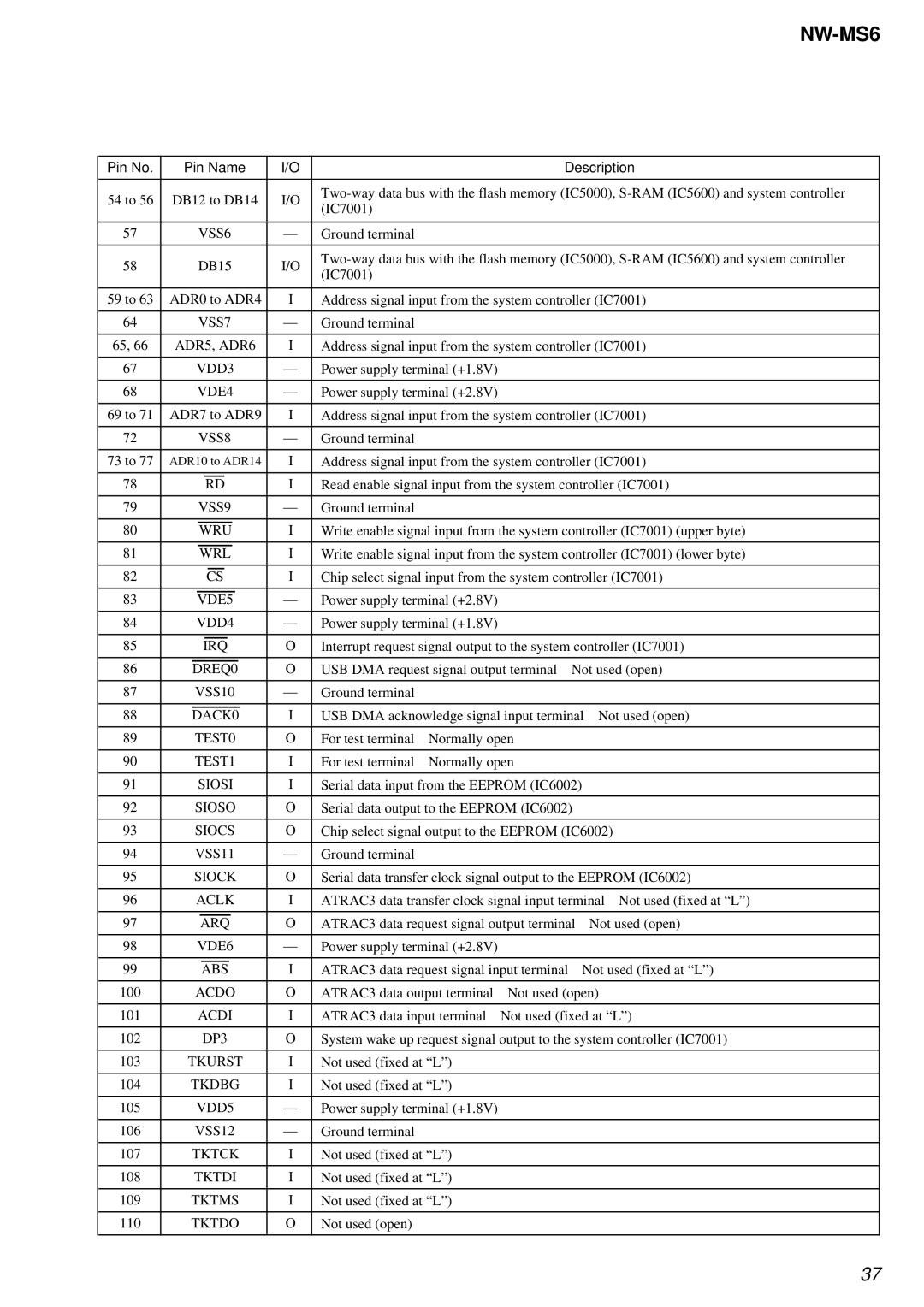
Pin No. | Pin Name | I/O |
|
| Description | ||||
|
|
|
|
|
| ||||
54 to 56 | DB12 to DB14 | I/O | |||||||
(IC7001) |
|
|
|
| |||||
|
|
|
|
|
|
|
|
| |
|
|
|
|
|
|
|
|
|
|
57 |
| VSS6 | — | Ground terminal |
|
|
|
| |
|
|
|
|
|
| ||||
58 |
| DB15 | I/O | ||||||
| (IC7001) |
|
|
|
| ||||
|
|
|
|
|
|
|
|
| |
|
|
|
|
|
| ||||
59 to 63 | ADR0 to ADR4 | I | Address signal input from the system controller (IC7001) | ||||||
|
|
|
|
|
|
|
|
|
|
64 |
| VSS7 | — | Ground terminal |
|
|
|
| |
|
|
|
|
|
| ||||
65, 66 | ADR5, ADR6 | I | Address signal input from the system controller (IC7001) | ||||||
|
|
|
|
|
|
|
|
| |
67 |
| VDD3 | — | Power supply terminal (+1.8V) |
|
|
| ||
|
|
|
|
|
|
|
|
| |
68 |
| VDE4 | — | Power supply terminal (+2.8V) |
|
|
| ||
|
|
|
|
|
| ||||
69 to 71 | ADR7 to ADR9 | I | Address signal input from the system controller (IC7001) | ||||||
|
|
|
|
|
|
|
|
|
|
72 |
| VSS8 | — | Ground terminal |
|
|
|
| |
|
|
|
|
|
| ||||
73 to 77 | ADR10 to ADR14 | I | Address signal input from the system controller (IC7001) | ||||||
|
|
|
|
|
| ||||
78 |
| RD | I | Read enable signal input from the system controller (IC7001) | |||||
|
|
|
|
|
|
|
|
| |
79 |
| VSS9 | — | Ground terminal |
|
|
|
| |
|
|
|
|
|
| ||||
80 |
| WRU | I | Write enable signal input from the system controller (IC7001) (upper byte) | |||||
|
|
|
|
|
| ||||
81 |
| WRL | I | Write enable signal input from the system controller (IC7001) (lower byte) | |||||
|
|
|
|
|
| ||||
82 |
| CS | I | Chip select signal input from the system controller (IC7001) | |||||
|
|
|
|
|
|
|
|
| |
83 |
| VDE5 | — | Power supply terminal (+2.8V) |
|
|
| ||
|
|
|
|
|
|
|
|
| |
84 |
| VDD4 | — | Power supply terminal (+1.8V) |
|
|
| ||
|
|
|
|
|
| ||||
85 |
| IRQ | O | Interrupt request signal output to the system controller (IC7001) | |||||
|
|
|
|
|
|
| |||
86 |
| DREQ0 | O | USB DMA request signal output terminal | Not used (open) | ||||
|
|
|
|
|
|
|
|
|
|
87 |
| VSS10 | — | Ground terminal |
|
|
|
| |
|
|
|
|
|
|
| |||
88 |
| DACK0 | I | USB DMA acknowledge signal input terminal | Not used (open) | ||||
|
|
|
|
|
|
|
|
| |
89 |
| TEST0 | O | For test terminal | Normally open |
|
| ||
|
|
|
|
|
|
|
| ||
90 |
| TEST1 | I | For test terminal | Normally open |
|
| ||
|
|
|
|
|
| ||||
91 |
| SIOSI | I | Serial data input from the EEPROM (IC6002) |
| ||||
|
|
|
|
|
| ||||
92 |
| SIOSO | O | Serial data output to the EEPROM (IC6002) |
| ||||
|
|
|
|
| |||||
93 |
| SIOCS | O | Chip select signal output to the EEPROM (IC6002) | |||||
|
|
|
|
|
|
|
|
| |
94 |
| VSS11 | — | Ground terminal |
|
|
|
| |
|
|
|
|
| |||||
95 |
| SIOCK | O | Serial data transfer clock signal output to the EEPROM (IC6002) | |||||
|
|
|
|
| |||||
96 |
| ACLK | I | ATRAC3 data transfer clock signal input terminal Not used (fixed at “L”) | |||||
|
|
|
|
|
|
| |||
97 |
| ARQ | O | ATRAC3 data request signal output terminal | Not used (open) | ||||
|
|
|
|
|
|
|
|
| |
98 |
| VDE6 | — | Power supply terminal (+2.8V) |
|
|
| ||
|
|
|
|
|
|
| |||
99 |
| ABS | I | ATRAC3 data request signal input terminal | Not used (fixed at “L”) | ||||
|
|
|
|
|
| ||||
100 |
| ACDO | O | ATRAC3 data output terminal | Not used (open) | ||||
|
|
|
|
|
| ||||
101 |
| ACDI | I | ATRAC3 data input terminal | Not used (fixed at “L”) | ||||
|
|
|
|
| |||||
102 |
| DP3 | O | System wake up request signal output to the system controller (IC7001) | |||||
|
|
|
|
|
|
|
| ||
103 |
| TKURST | I | Not used (fixed at “L”) |
|
|
| ||
|
|
|
|
|
|
|
| ||
104 |
| TKDBG | I | Not used (fixed at “L”) |
|
|
| ||
|
|
|
|
|
|
|
| ||
105 |
| VDD5 | — | Power supply terminal (+1.8V) |
|
|
| ||
|
|
|
|
|
|
|
|
| |
106 |
| VSS12 | — | Ground terminal |
|
|
|
| |
|
|
|
|
|
|
|
| ||
107 |
| TKTCK | I | Not used (fixed at “L”) |
|
|
| ||
|
|
|
|
|
|
|
| ||
108 |
| TKTDI | I | Not used (fixed at “L”) |
|
|
| ||
|
|
|
|
|
|
|
| ||
109 |
| TKTMS | I | Not used (fixed at “L”) |
|
|
| ||
|
|
|
|
|
|
|
|
| |
110 |
| TKTDO | O | Not used (open) |
|
|
|
| |
|
|
|
|
|
|
|
|
|
|
37