Step 3. Configure Memory
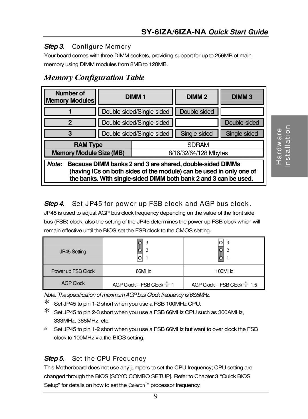
Your board comes with three DIMM sockets, providing support for up to 256MB of main memory using DIMM modules from 8MB to 128MB.
Memory Configuration Table
|
|
|
|
|
|
|
|
|
|
|
|
|
| Number of |
|
| DIMM 1 |
| DIMM 2 |
| DIMM 3 |
|
|
| |
| Memory Modules |
|
|
|
|
|
|
| ||||
|
|
|
|
|
|
|
|
|
|
|
| |
|
|
|
|
|
|
|
|
|
|
|
| |
| 1 |
|
|
|
|
|
|
| ||||
| 2 |
|
|
|
|
|
| Hardware Installation | ||||
|
|
|
|
|
|
|
|
|
|
| ||
| Note: Because | DIMM banks 2 and 3 are shared, |
| DIMMs |
|
| ||||||
| 3 |
|
|
|
|
|
| |||||
| RAM Type |
|
|
| SDRAM |
|
|
|
|
| ||
| Memory Module Size (MB) |
| 8/16/32/64/128 Mbytes |
|
|
| ||||||
|
|
|
| |||||||||
| (having ICs on both sides of the module) can be used in only one of |
|
|
| ||||||||
| the banks. With |
|
|
| ||||||||
|
| |||||||||||
|
|
|
|
|
|
|
|
|
|
|
|
|
Step 4. Set JP45 for power up FSB clock and AGP bus clock.
JP45 is used to adjust AGP bus clock frequency depending on the value of the front side bus (FSB) clock, also the setting of the JP45 determines the power up FSB clock which will remain effective until the BIOS set the FSB clock to the CMOS setting.
|
| 3 |
| 3 |
|
|
| ||
|
|
| ||
JP45 Setting |
| 2 |
| 2 |
|
| |||
|
| |||
|
| 1 |
| 1 |
|
| |||
|
|
|
|
|
Power up FSB Clock | 66MHz | 100MHz | ||
|
|
|
|
|
AGP Clock | AGP Clock = FSB Clock ÷ 1 | AGP Clock = FSB Clock ÷ 1.5 | ||
|
|
|
|
|
Note: The specification of maximum AGP bus Clock frequency is 66.6MHz.
∗Set JP45 to pin 1-2 short when you use a FSB 100MHz CPU.
∗Set JP45 to pin
∗Set JP45 to pin
Step 5. Set the CPU Frequency
This Motherboard does not use any jumpers to set the CPU frequency; CPU setting are changed through the BIOS [SOYO COMBO SETUP]. Refer to Chapter 3 “Quick BIOS Setup”for details on how to set the CeleronTM processor frequency.
9
