Software Control | www.ti.com |
•FIFO: allows the configuration of the FIFO and FIFO sync sources.
•LVDS delay: provides internal delay of either the LVDS DATA or LVDS DATACLK to help meet the input setup/hold time.
•Data Routing: provides flexible routing of the A, B, C, and D sample input data to the appropriate digital path.
Note: the DAC3482 does not support this mode
•SIF Control: provides control of the Serial Interface
•Input Format: provides control of the input data format (i.e., 2’s complement or offset binary).
•Parity: provides configuration of the parity input.
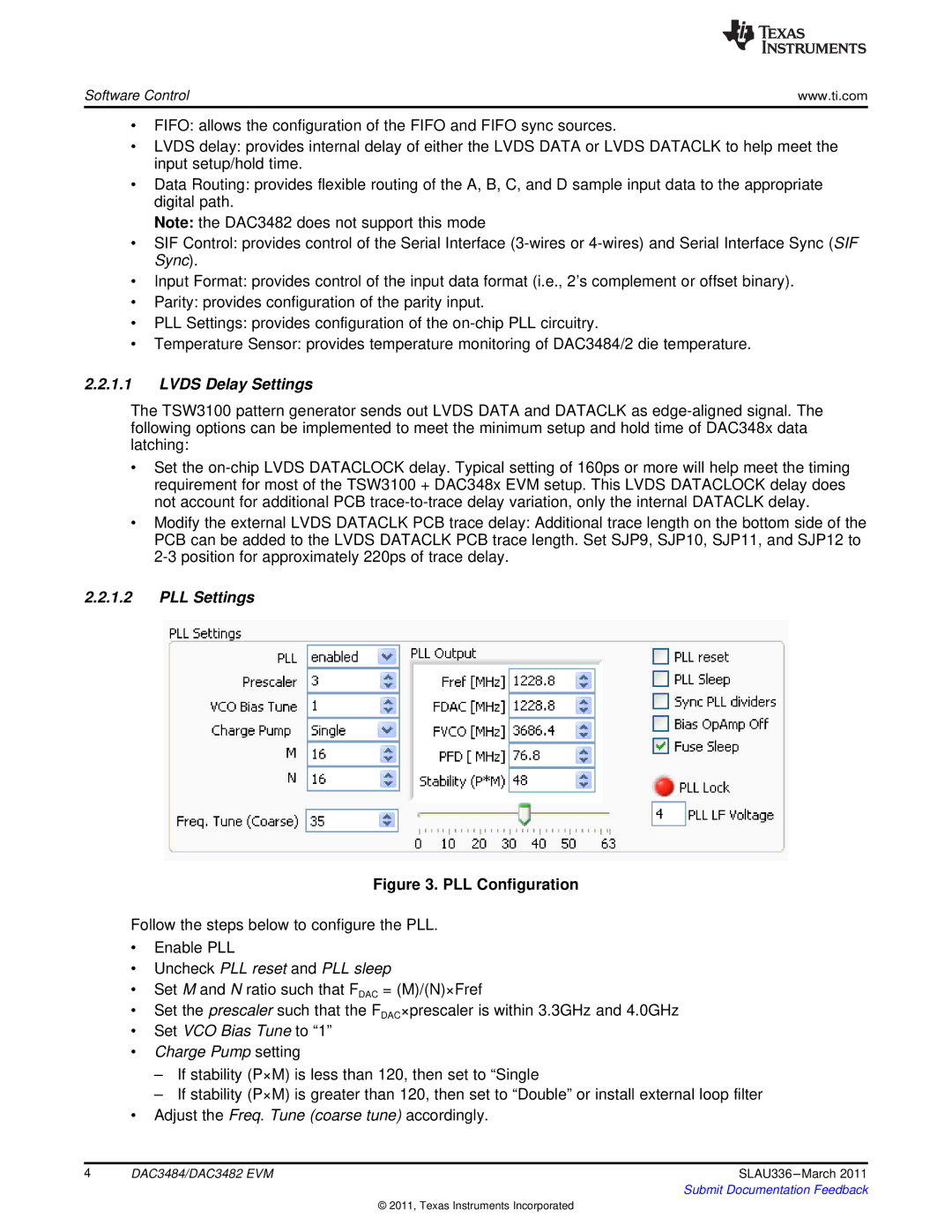
•PLL Settings: provides configuration of the
•Temperature Sensor: provides temperature monitoring of DAC3484/2 die temperature.
2.2.1.1LVDS Delay Settings
The TSW3100 pattern generator sends out LVDS DATA and DATACLK as
•Set the
•Modify the external LVDS DATACLK PCB trace delay: Additional trace length on the bottom side of the PCB can be added to the LVDS DATACLK PCB trace length. Set SJP9, SJP10, SJP11, and SJP12 to
2.2.1.2PLL Settings
Figure 3. PLL Configuration
Follow the steps below to configure the PLL.
•Enable PLL
•Uncheck PLL reset and PLL sleep
•Set M and N ratio such that FDAC = (M)/(N)×Fref
•Set the prescaler such that the FDAC×prescaler is within 3.3GHz and 4.0GHz
•Set VCO Bias Tune to “1”
•Charge Pump setting
–If stability (P×M) is less than 120, then set to “Single
–If stability (P×M) is greater than 120, then set to “Double” or install external loop filter
•Adjust the Freq. Tune (coarse tune) accordingly.
4 | DAC3484/DAC3482 EVM | SLAU336 |
|
| Submit Documentation Feedback |
© 2011, Texas Instruments Incorporated
