www.ti.com | Software Control |
2.2.4CDCE62005
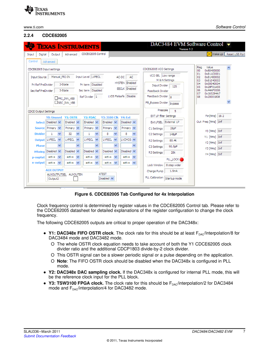
Figure 6. CDCE62005 Tab Configured for 4x Interpolation
Clock frequency control is determined by register values in the CDCE62005 Control tab. Please refer to the CDCE62005 datasheet for detailed explanations of the register configuration to change the clock frequency.
The following CDCE62005 outputs are critical to proper operation of the DAC348x:
●Y1: DAC348x FIFO OSTR clock. The clock rate for this should be at least FDAC/Interpolation/8 for DAC3484 mode and DAC3482 mode.
OThe whole OSTR clock equation needs to take account of both the Y1 CDCE62005 clock divider ratio and the additional CDCP1803
O This OSTR signal can be a slower periodic signal or a pulse depending on the application.
ONote: The FIFO OSTR clock should be disabled when the DAC348x is configured in PLL mode.
●Y2: DAC348x DAC sampling clock. If the DAC348x is configured for internal PLL mode, this will be the reference clock input for the PLL block.
●Y3: TSW3100 FPGA clock. The clock rate for this should be FDAC/interpolation/2 for DAC3484 mode and FDAC/interpolation/4 for DAC3482 mode.
SLAU336 | DAC3484/DAC3482 EVM | 7 |
Submit Documentation Feedback |
|
|
© 2011, Texas Instruments Incorporated