Introduction | www.ti.com |
1 Introduction
1.1Overview
This document is intended to serve as a basic user’s guide for the DAC3484/2 EVM Revision D. The EVM provides a basic platform to evaluate the DAC3484 and DAC3482, which are a family of 1.25GSPS, up to 16x interpolation,
The EVM includes the CDCE62005 clocking source which provides the clocks required for the DAC and the pattern generator. The
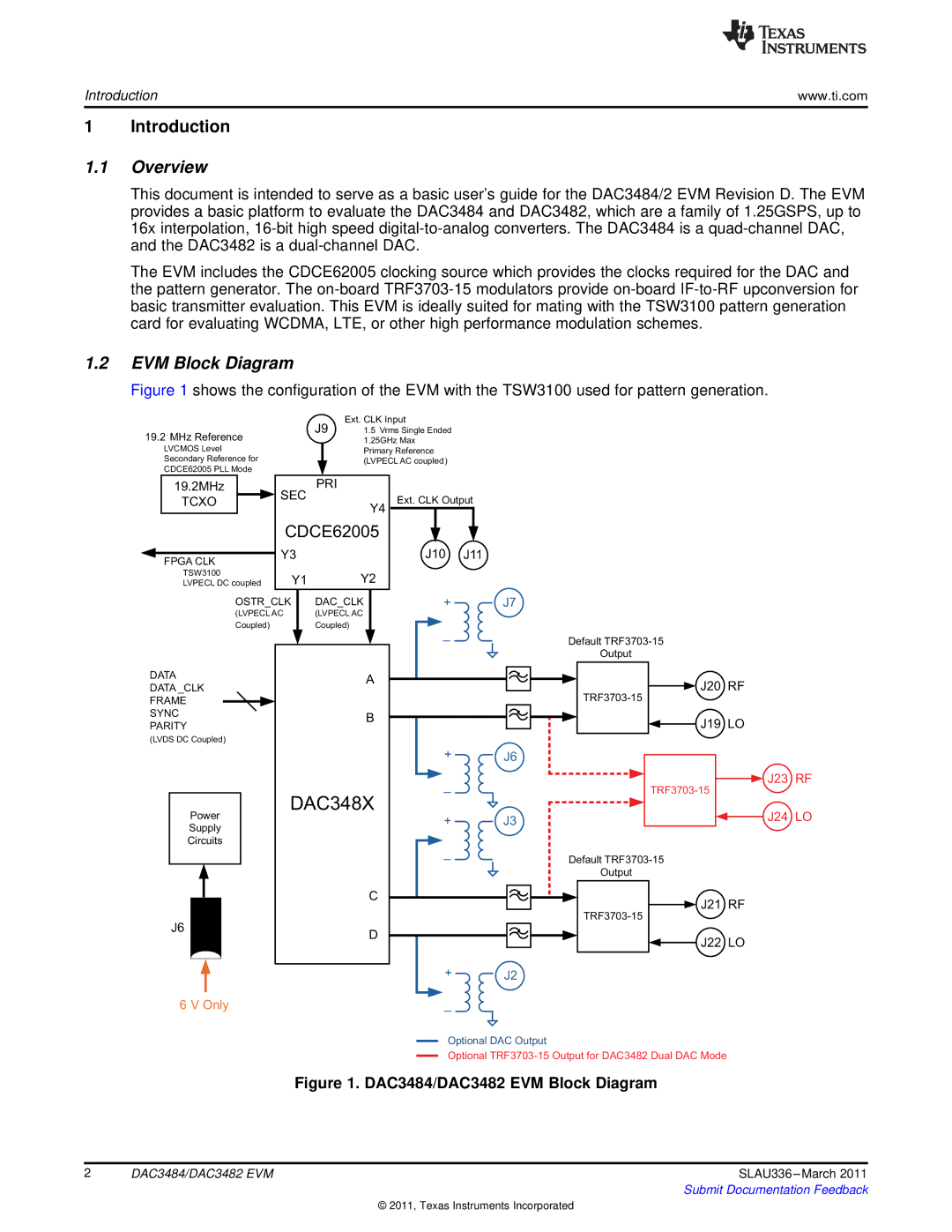
1.2EVM Block Diagram
Figure 1 shows the configuration of the EVM with the TSW3100 used for pattern generation.
19.2 MHz Reference
LVCMOS Level Secondary Reference for CDCE62005 PLL Mode
J9 | Ext. CLK Input |
1.5 Vrms Single Ended | |
| 1.25GHz Max |
| Primary Reference |
| (LVPECL AC coupled ) |
19.2MHz | SEC | PRI |
TCXO |
| |
| Y4 | |
|
| |
| CDCE62005 | |
FPGA CLK | Y3 |
|
|
| |
TSW3100 | Y1 | Y2 |
LVPECL DC coupled | ||
OSTR_CLK | DAC_CLK | |
(LVPECL AC | (LVPECL AC | |
Coupled) |
| Coupled) |
Ext. CLK Output
J10 J11
+ | J7 |
_ |
|
Default
Output
DATA
DATA _CLK
FRAME
SYNC
PARITY
(LVDS DC Coupled)
Power
Supply
Circuits
J6
A
B
DAC348X
C
D
+ | J6 |
_ |
|
+ | J3 |
_ |
|
+ | J2 |
![]() J20 RF
J20 RF
J19 LO
![]() J23 RF
J23 RF
J24 LO
Default
Output
![]() J21 RF
J21 RF
J22 LO
6 V Only | _ |
Optional DAC Output
Optional
Figure 1. DAC3484/DAC3482 EVM Block Diagram
2 | DAC3484/DAC3482 EVM | SLAU336 |
|
| Submit Documentation Feedback |
© 2011, Texas Instruments Incorporated