www.ti.com
Schematics and Layout
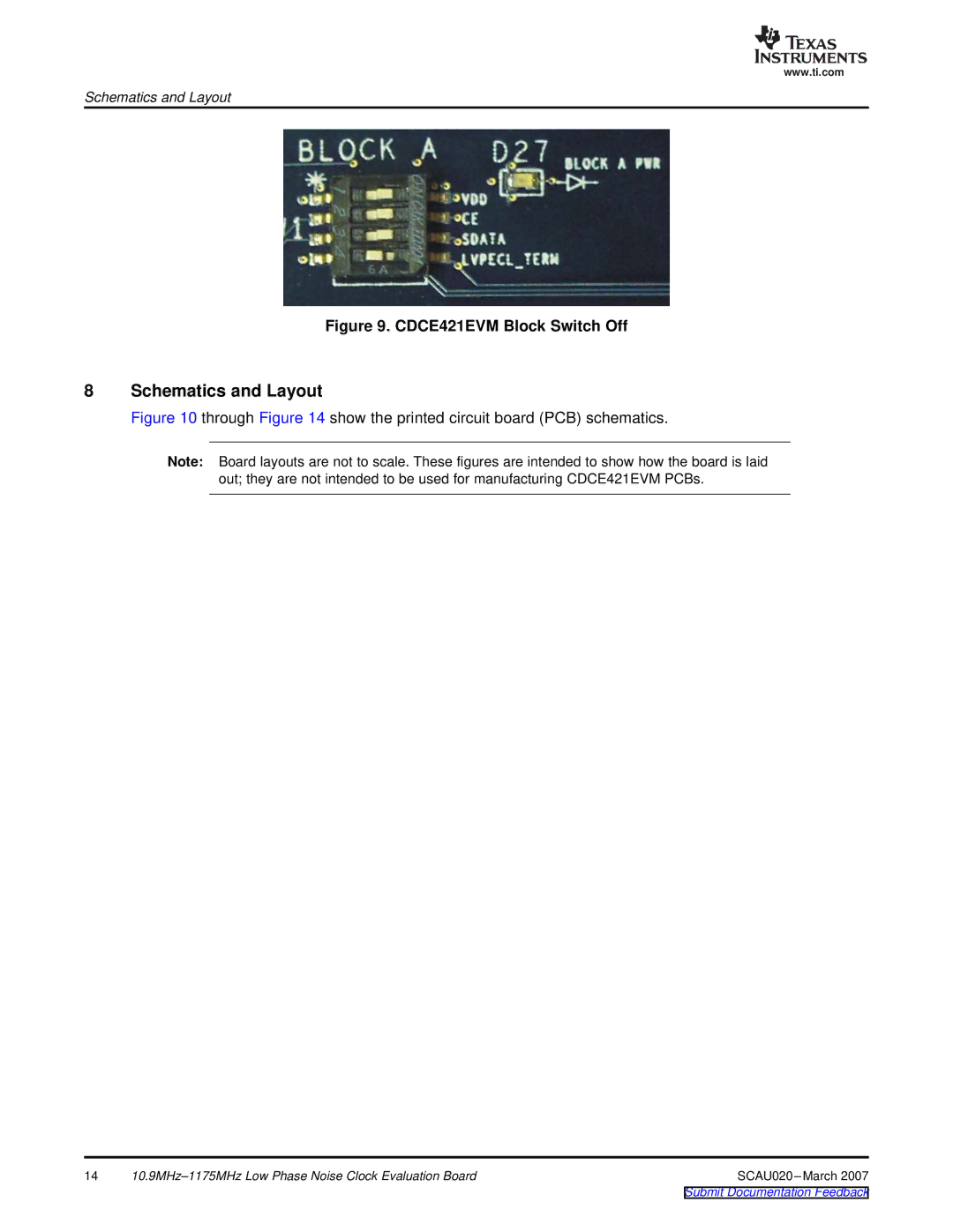
Figure 9. CDCE421EVM Block Switch Off
8Schematics and Layout
Figure 10 through Figure 14 show the printed circuit board (PCB) schematics.
Note: Board layouts are not to scale. These figures are intended to show how the board is laid out; they are not intended to be used for manufacturing CDCE421EVM PCBs.
14 | SCAU020 |
