www.ti.com
ChronosGUI
frequency should be entered here in this format: xx.xxx (specified in MHz).
Step 3. Output Calculator and Apply PLL Settings.
The second row of calculations is used to obtain the PLL settings necessary to achieve a particular output frequency provided a given input frequency to CDCE421. The input must be entered in the second row as well as the location provided at the input of the PLL block diagram. After the Calculate button is pressed, the adjacent
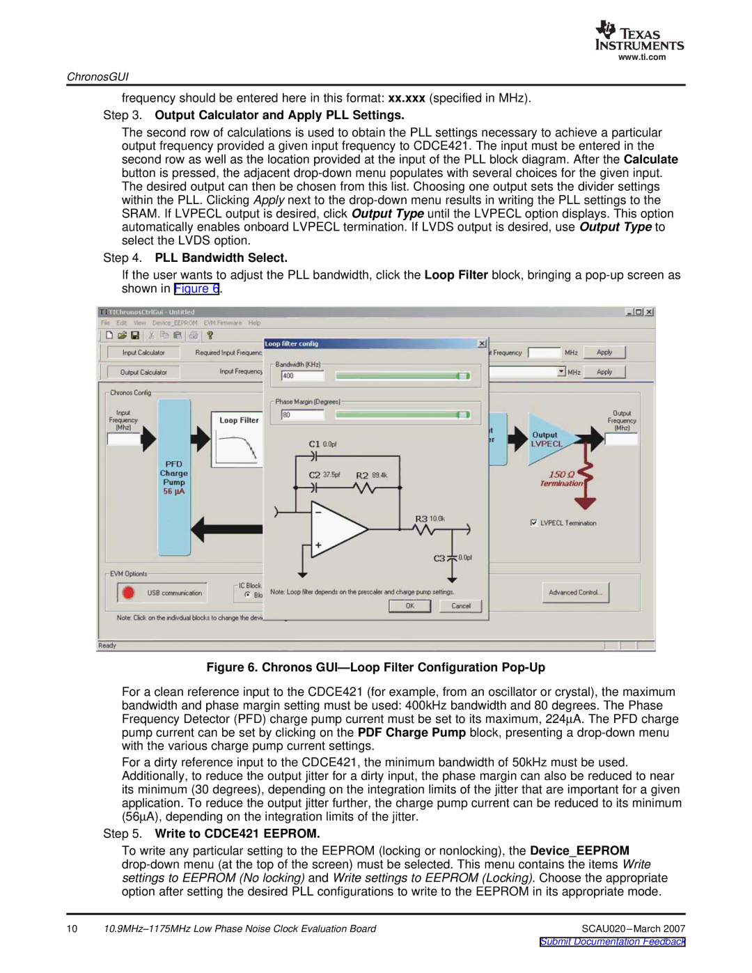
Step 4. PLL Bandwidth Select.
If the user wants to adjust the PLL bandwidth, click the Loop Filter block, bringing a
Figure 6. Chronos GUI—Loop Filter Configuration Pop-Up
For a clean reference input to the CDCE421 (for example, from an oscillator or crystal), the maximum bandwidth and phase margin setting must be used: 400kHz bandwidth and 80 degrees. The Phase Frequency Detector (PFD) charge pump current must be set to its maximum, 224μA. The PFD charge pump current can be set by clicking on the PDF Charge Pump block, presenting a
For a dirty reference input to the CDCE421, the minimum bandwidth of 50kHz must be used. Additionally, to reduce the output jitter for a dirty input, the phase margin can also be reduced to near its minimum (30 degrees), depending on the integration limits of the jitter that are important for a given application. To reduce the output jitter further, the charge pump current can be reduced to its minimum (56μA), depending on the integration limits of the jitter.
Step 5. Write to CDCE421 EEPROM.
To write any particular setting to the EEPROM (locking or nonlocking), the Device_EEPROM
10 | SCAU020 |