www.ti.com
Signal Path and Control Circuitry
2Signal Path and Control Circuitry
The CDCE421 can accept a
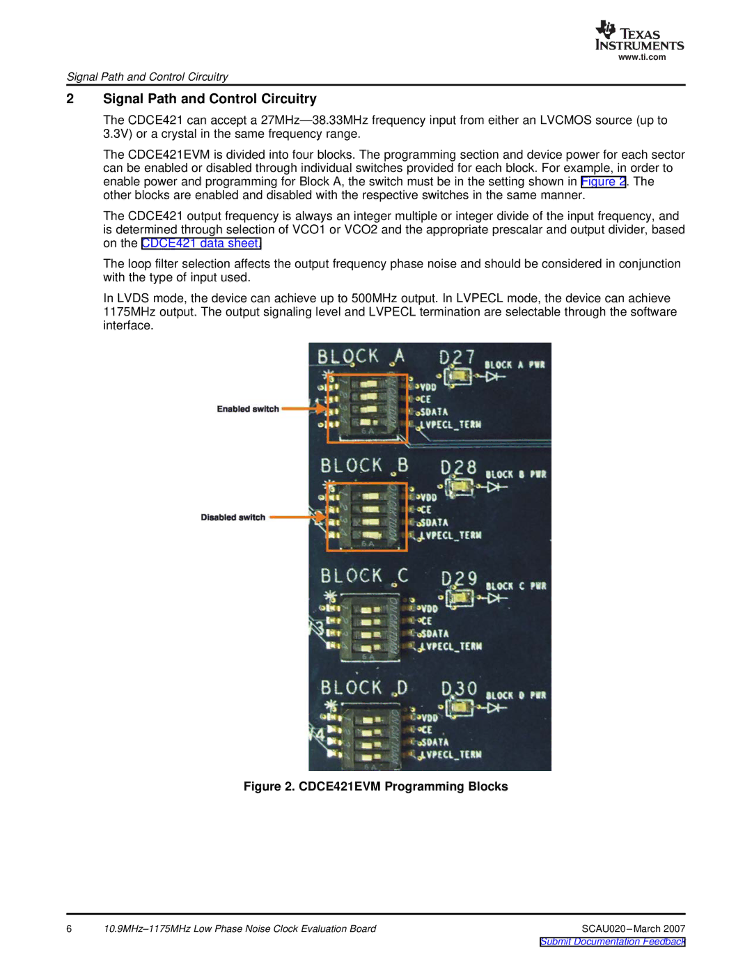
The CDCE421EVM is divided into four blocks. The programming section and device power for each sector can be enabled or disabled through individual switches provided for each block. For example, in order to enable power and programming for Block A, the switch must be in the setting shown in Figure 2. The other blocks are enabled and disabled with the respective switches in the same manner.
The CDCE421 output frequency is always an integer multiple or integer divide of the input frequency, and is determined through selection of VCO1 or VCO2 and the appropriate prescalar and output divider, based on the CDCE421 data sheet.
The loop filter selection affects the output frequency phase noise and should be considered in conjunction with the type of input used.
In LVDS mode, the device can achieve up to 500MHz output. In LVPECL mode, the device can achieve 1175MHz output. The output signaling level and LVPECL termination are selectable through the software interface.
Figure 2. CDCE421EVM Programming Blocks
6 | SCAU020 |