AR-B1375/AR-B1376 User s Guide

9. USING MEMORY BANKS

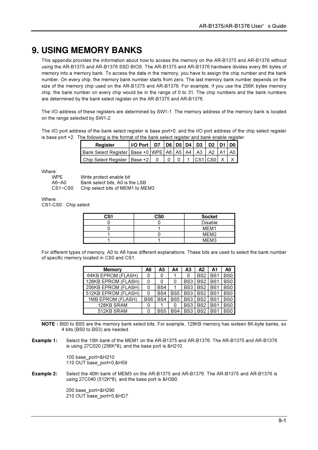
This appendix provides the information about how to access the memory on the AR-B1375 and AR-B1376 without using the AR-B1375 and AR-B1376 SSD BIOS. The AR-B1375 and AR-B1376 hardware divides every 8K bytes of memory into a memory bank. To access the data in the memory, you have to assign the chip number and the bank number. On every chip, the memory bank number starts from zero. The last memory bank number depends on the size of the memory chip used on the AR-B1375 and AR-B1376. For example, if you use the 256K bytes memory chip, the bank number on every chip would be in the range of 0 to 31. The chip numbers and the bank numbers are determined by the bank select register on the AR-B1375 and AR-B1376.

The I/O address of these registers are determined by SW1-1. The memory address of the memory bank is located on the range selected by SW1-2.

The I/O port address of the bank select register is base port+0, and the I/O port address of the chip select register is base port +2. The following is the format of the bank select register and bank enable register.


Register


I/O Port

D7

D6

D5

D4

D3


D2

D1

D0


Bank Select Register


Base +0

WPE

A6

A5

A4

A3


A2

A1

A0


Chip Select Register


Base +2

0

0

0

1

CS1

CS0

X

X

Where:


WPE

Write protect enable bit


A6~A0

Bank select bits, A0 is the LSB


CS1~CS0

Chip select bits of MEM1 to MEM3


Where:


CS1-CS0 : Chip select


CS1


CS0


Socket


0


0


Disable


0


1


MEM1


1


0


MEM2


1


1


MEM3


For different types of memory, A0 to A6 have different explanations. These bits are used to select the bank number of specific memory located in CS0 and CS1.

Memory

A6

A5

A4

A3

A2

A1

A0

64KB EPROM (FLASH)

0

0

1

0

BS2

BS1

BS0

128KB EPROM (FLASH)

0

0

0

BS3

BS2

BS1

BS0

256KB EPROM (FLASH)

0

BS4

1

BS3

BS2

BS1

BS0

512KB EPROM (FLASH)

0

BS4

BS5

BS3

BS2

BS1

BS0

1MB EPROM (FLASH)

BS6

BS4

BS5

BS3

BS2

BS1

BS0

128KB SRAM

0

1

0

BS3

BS2

BS1

BS0

512KB SRAM

0

BS5

BS4

BS3

BS2

BS1

BS0

NOTE : BS0 to BS5 are the memory bank select bits. For example, 128KB memory has sixteen 8K-byte banks, so 4 bits (BS0 to BS3) are needed.

Example 1: Select the 10th bank of the MEM1 on the AR-B1375 and AR-B1376. The AR-B1375 and AR-B1376 is using 27C020 (256K*8), and the base port is &H210.

100 base_port=&H210

110 OUT base_port+0,&H59

Example 2: Select the 40th bank of MEM3 on the AR-B1375 and AR-B1376. The AR-B1375 and AR-B1376 is using 27C040 (512K*8), and the base port is &H390.

200 base_port=&H290

210 OUT base_port+0,&HD7

9-1

Page 63
Image 63
Toshiba AR-B1376, AR-B1375, 386SX manual Using Memory Banks, Register Port, CS1 CS0, Socket

386SX, AR-B1376, AR-B1375 specifications

The Toshiba AR-B1375 and AR-B1376 are notable embedded computing solutions that incorporate the 386SX microprocessor architecture. Designed for various applications, these models focus on reliability, performance, and versatility, making them appealing choices for system integrators and developers.

At the core of the AR-B1375 and AR-B1376 is the Intel 386SX microprocessor. This landmark processor marked a significant advancement in computing technology, introducing a 32-bit architecture while maintaining compatibility with 16-bit applications. The 386SX is known for its efficient processing capabilities, offering both multitasking support and enhanced memory management. It operates at clock speeds ranging typically from 16 MHz to 25 MHz, contributing to its effectiveness in running industrial applications.

One of the key features of the AR-B1375 and AR-B1376 systems is their modular architecture, which allows for easy customization and expansion. This modularity means users can tailor the hardware according to specific requirements, making it suitable for a wide range of applications such as automation, telecommunications, and embedded systems.

Both models support various I/O options, ensuring seamless integration with peripherals and external devices. They typically come equipped with serial and parallel ports, as well as support for modern interfaces like USB. The systems also feature onboard expansion slots, enabling the addition of further functionality, such as additional memory or specialized processing units.

In terms of memory, the AR-B1375 and AR-B1376 support a range of RAM configurations, allowing users to scale their systems based on the application demands. The inclusion of EPROM and EEPROM options also facilitates easy updates and programmability, which is crucial for embedded systems that often require firmware adjustments over time.

Moreover, these models are known for their robust thermal management features, which are essential in industrial environments where conditions can be harsh. This capability ensures stable performance and longevity, reducing the risk of system failures due to overheating or environmental factors.

To summarize, the Toshiba AR-B1375 and AR-B1376, coupled with the 386SX microprocessor, offer a blend of performance, flexibility, and reliability. Their modular design, extensive I/O support, and memory scalability make them ideal for a variety of embedded computing applications, placing them as commendable options in the world of industrial computing solutions. These systems not only exemplify Toshiba's commitment to innovation but also contribute significantly to the functionality of embedded technologies in a rapidly evolving industry.