YMF724F
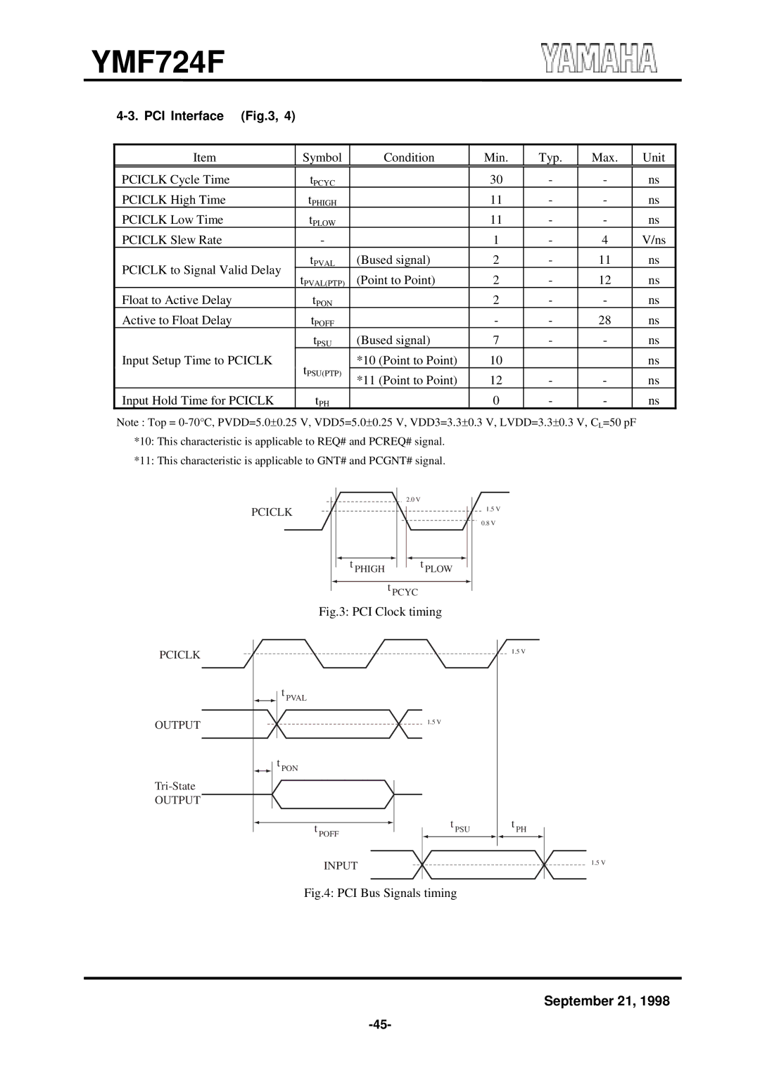
4-3. PCI Interface (Fig.3, 4)
Item | Symbol | Condition | Min. | Typ. | Max. | Unit | |
|
|
|
|
|
|
| |
PCICLK Cycle Time | tPCYC |
| 30 | - | - | ns | |
PCICLK High Time | tPHIGH |
| 11 | - | - | ns | |
PCICLK Low Time | tPLOW |
| 11 | - | - | ns | |
PCICLK Slew Rate | - |
| 1 | - | 4 | V/ns | |
PCICLK to Signal Valid Delay | tPVAL | (Bused signal) | 2 | - | 11 | ns | |
tPVAL(PTP) | (Point to Point) | 2 | - | 12 | ns | ||
| |||||||
Float to Active Delay | tPON |
| 2 | - | - | ns | |
Active to Float Delay | tPOFF |
| - | - | 28 | ns | |
| tPSU | (Bused signal) | 7 | - | - | ns | |
Input Setup Time to PCICLK | tPSU(PTP) | *10 (Point to Point) | 10 |
|
| ns | |
| *11 (Point to Point) | 12 | - | - | ns | ||
|
| ||||||
Input Hold Time for PCICLK | tPH |
| 0 | - | - | ns |
Note : Top =
*11: This characteristic is applicable to GNT# and PCGNT# signal.
|
| 2.0 V | ||
PCICLK |
|
| 1.5 V | |
|
|
| ||
|
|
|
| 0.8 V |
|
|
|
|
|
t PHIGH |
| t PLOW | ||
t PCYC
PCICLK
OUTPUT
OUTPUT
Fig.3: PCI Clock timing
1.5 V
tPVAL
1.5 V
tPON
|
|
|
| t PSU |
| t PH |
t | POFF | |||||
|
|
|
|
| ||
INPUT | 1.5 V |
|
Fig.4: PCI Bus Signals timing
September 21, 1998