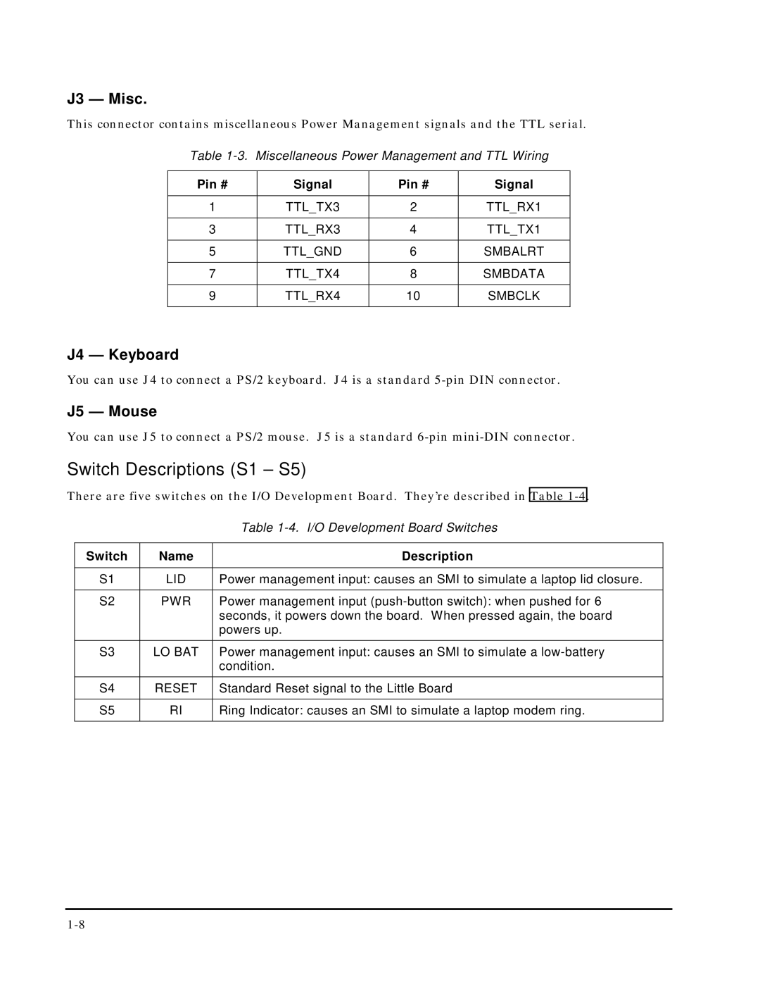
5001451A specifications
Ampro Corporation is known for its commitment to quality and innovation, particularly in the field of embedded computing solutions. One of its standout products, the Ampro Corporation 5001451A, is a robust and versatile embedded computing platform designed to meet the demanding needs of industrial applications.The 5001451A features a compact and modular design that allows for flexibility and ease of integration into various systems. It is built around a powerful processor, ensuring high performance for data-intensive operations. This embedded platform can support various operating systems, giving developers the freedom to choose the environment that best suits their project requirements. Additionally, the system's architecture is optimized for low power consumption, which is critical for applications where energy efficiency is paramount.
One of the key characteristics of the 5001451A is its extensive I/O capabilities. It includes multiple ports for serial communication, USB, and Ethernet, making it highly adaptable for different connectivity needs. The system also supports various expansion options, allowing users to add additional functionalities as required. This adaptability is essential for industries such as telecommunications, transportation, and medical devices, where specific operational demands vary widely.
Moreover, the 5001451A is designed with durability in mind. It can operate effectively in challenging environments, with features such as extended temperature ranges and resistance to shock and vibration. This ruggedness makes it an ideal choice for deployment in outdoor installations or industrial settings where equipment is subjected to harsh conditions.
The product also integrates advanced security features to protect against cyber threats, which is increasingly important in today's connected world. With built-in encryption and secure boot capabilities, the 5001451A ensures that sensitive data is safe and that the system remains reliable against unauthorized access.
In summary, the Ampro Corporation 5001451A stands out as a powerful, flexible, and reliable embedded computing solution. Its combination of performance, modularity, durability, and security makes it an excellent choice for a wide range of industrial applications, making it a go-to option for developers and engineers seeking a dependable embedded platform. With the ongoing advancements in technology, the 5001451A is well-positioned to adapt to future challenges and opportunities in the ever-evolving landscape of embedded systems.