AD9843A

together with CLPOB or separately. The CLPDM pulse should be a minimum of four pixels wide.

Variable Gain Amplifier

The VGA stage provides a gain range of 2 dB to 36 dB, program- mable with 10-bit resolution through the serial digital interface. Combined with the typical 4 dB gain from the CDS stage, the total gain range for the AD9843A is 6 dB to 40 dB. A gain of

6dB will match a 1 V input signal with the ADC full-scale range of

2V. When compared to 1 V full-scale systems (such as ADI’s AD9803), the equivalent gain range is 0 dB to 34 dB.

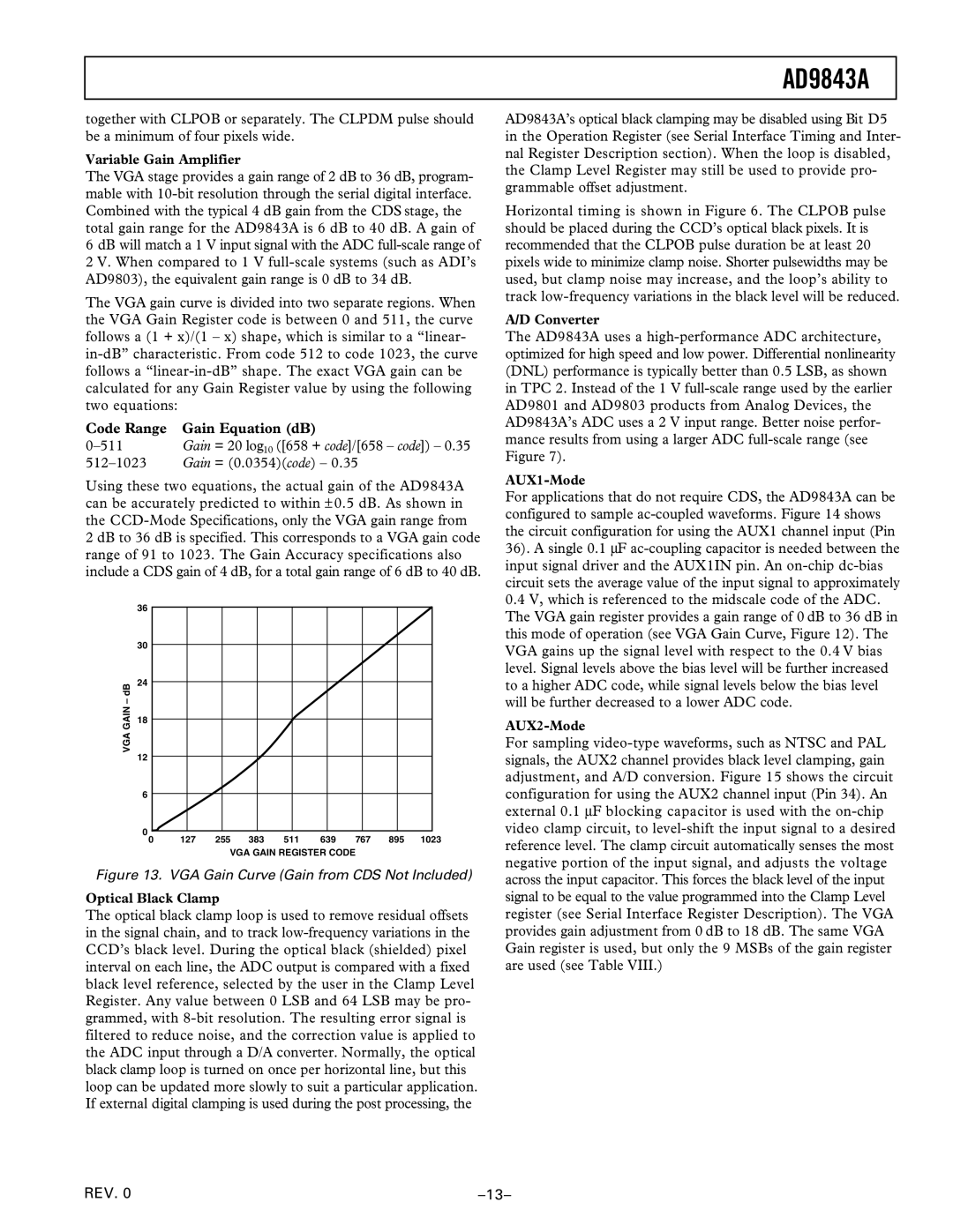
The VGA gain curve is divided into two separate regions. When the VGA Gain Register code is between 0 and 511, the curve follows a (1 + x)/(1 – x) shape, which is similar to a “linear- in-dB” characteristic. From code 512 to code 1023, the curve follows a “linear-in-dB” shape. The exact VGA gain can be calculated for any Gain Register value by using the following two equations:

Code Range

Gain Equation (dB)

0–511

Gain = 20 log10 ([658 + code]/[658 – code]) – 0.35

512–1023

Gain = (0.0354)(code) – 0.35

Using these two equations, the actual gain of the AD9843A can be accurately predicted to within ± 0.5 dB. As shown in the CCD-Mode Specifications, only the VGA gain range from

2 dB to 36 dB is specified. This corresponds to a VGA gain code range of 91 to 1023. The Gain Accuracy specifications also include a CDS gain of 4 dB, for a total gain range of 6 dB to 40 dB.


36


30

– dB

24


GAINVGA

18


12


6


0

0 127 255 383 511 639 767 895 1023

VGA GAIN REGISTER CODE

Figure 13. VGA Gain Curve (Gain from CDS Not Included)

Optical Black Clamp

The optical black clamp loop is used to remove residual offsets in the signal chain, and to track low-frequency variations in the CCD’s black level. During the optical black (shielded) pixel interval on each line, the ADC output is compared with a fixed black level reference, selected by the user in the Clamp Level Register. Any value between 0 LSB and 64 LSB may be pro- grammed, with 8-bit resolution. The resulting error signal is filtered to reduce noise, and the correction value is applied to the ADC input through a D/A converter. Normally, the optical black clamp loop is turned on once per horizontal line, but this loop can be updated more slowly to suit a particular application. If external digital clamping is used during the post processing, the

AD9843A’s optical black clamping may be disabled using Bit D5 in the Operation Register (see Serial Interface Timing and Inter- nal Register Description section). When the loop is disabled, the Clamp Level Register may still be used to provide pro- grammable offset adjustment.

Horizontal timing is shown in Figure 6. The CLPOB pulse should be placed during the CCD’s optical black pixels. It is recommended that the CLPOB pulse duration be at least 20 pixels wide to minimize clamp noise. Shorter pulsewidths may be used, but clamp noise may increase, and the loop’s ability to track low-frequency variations in the black level will be reduced.

A/D Converter

The AD9843A uses a high-performance ADC architecture, optimized for high speed and low power. Differential nonlinearity (DNL) performance is typically better than 0.5 LSB, as shown in TPC 2. Instead of the 1 V full-scale range used by the earlier AD9801 and AD9803 products from Analog Devices, the AD9843A’s ADC uses a 2 V input range. Better noise perfor- mance results from using a larger ADC full-scale range (see Figure 7).

AUX1-Mode

For applications that do not require CDS, the AD9843A can be configured to sample ac-coupled waveforms. Figure 14 shows the circuit configuration for using the AUX1 channel input (Pin 36). A single 0.1 ∝F ac-coupling capacitor is needed between the input signal driver and the AUX1IN pin. An on-chip dc-bias circuit sets the average value of the input signal to approximately

0.4V, which is referenced to the midscale code of the ADC. The VGA gain register provides a gain range of 0 dB to 36 dB in this mode of operation (see VGA Gain Curve, Figure 12). The VGA gains up the signal level with respect to the 0.4 V bias level. Signal levels above the bias level will be further increased to a higher ADC code, while signal levels below the bias level will be further decreased to a lower ADC code.

AUX2-Mode

For sampling video-type waveforms, such as NTSC and PAL signals, the AUX2 channel provides black level clamping, gain adjustment, and A/D conversion. Figure 15 shows the circuit configuration for using the AUX2 channel input (Pin 34). An external 0.1 ∝F blocking capacitor is used with the on-chip video clamp circuit, to level-shift the input signal to a desired reference level. The clamp circuit automatically senses the most negative portion of the input signal, and adjusts the voltage across the input capacitor. This forces the black level of the input signal to be equal to the value programmed into the Clamp Level register (see Serial Interface Register Description). The VGA provides gain adjustment from 0 dB to 18 dB. The same VGA Gain register is used, but only the 9 MSBs of the gain register are used (see Table VIII.)

REV. 0

–13–

Page 13
Image 13
Analog Devices AD9843A manual Code Range Gain Equation dB

AD9843A specifications

The Analog Devices AD9843A is a high-performance, integrated analog-to-digital converter (ADC) designed for a variety of applications requiring precise signal conversion. This device boasts a 12-bit resolution, making it suitable for capturing fine details in complex signals. The AD9843A operates with a maximum sampling rate of up to 130 MSPS (mega samples per second), which allows it to handle fast-changing waveforms effectively, ideal for applications in the fields of telecommunications, instrumentation, and medical imaging.

One of the standout features of the AD9843A is its dual-channel architecture, which enables simultaneous sampling of two input signals. This capability is particularly beneficial in applications such as radar and sonar systems, where capturing multiple input sources in parallel is critical. Furthermore, the ADC incorporates a high-speed programmable gain amplifier (PGA), providing adjustable gain settings to accommodate a wide range of signal amplitudes, ensuring optimal performance across various input conditions.

The AD9843A employs Differential Non-Linearity (DNL) and Integral Non-Linearity (INL) specifications, both of which contribute to its impressive accuracy and linearity. With a DNL of ±0.5 LSB (least significant bit) and an INL of ±1 LSB, the AD9843A minimizes distortion and enhances the fidelity of the digital representation of analog signals. Additionally, the device features low noise performance, which is essential for obtaining high-quality signal digitization, especially in sensitive applications where signal integrity is paramount.

Another key characteristic is the integrated sample-and-hold circuit that allows the ADC to capture input signals with minimal distortion during the conversion process. This design choice helps to stabilize the input signal, reducing the effect of sampling jitter. The AD9843A also provides various output data formats, including binary, gray code, and two's complement, which gives designers the flexibility to interface the ADC with different digital systems.

In terms of power consumption, the AD9843A is efficient, operating at a typical supply voltage of 5V. It offers a significant advantage for battery-operated devices by ensuring that the power requirements are kept low without compromising performance. With its combination of high throughput, low noise, and versatility, the Analog Devices AD9843A stands out as a robust solution for high-speed data acquisition systems, making it a preferred choice among engineers and designers across various industries.