Using the STK502 Top Module
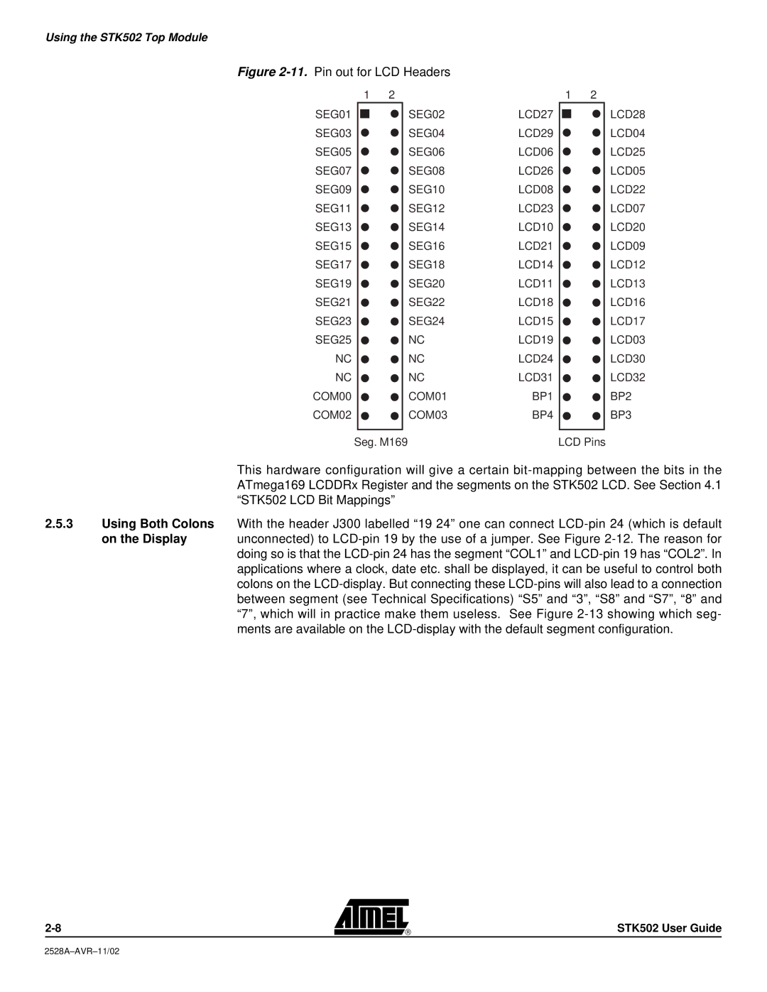
Figure 2-11. Pin out for LCD Headers
1 2
SEG01
SEG03
SEG05
SEG07
SEG09
SEG11
SEG13
SEG15
SEG17
SEG19
SEG21
SEG23
SEG25
NC
NC
COM00
COM02
1 2
SEG02 | LCD27 |
SEG04 | LCD29 |
SEG06 | LCD06 |
SEG08 | LCD26 |
SEG10 | LCD08 |
SEG12 | LCD23 |
SEG14 | LCD10 |
SEG16 | LCD21 |
SEG18 | LCD14 |
SEG20 | LCD11 |
SEG22 | LCD18 |
SEG24 | LCD15 |
NC | LCD19 |
NC | LCD24 |
NC | LCD31 |
COM01 | BP1 |
COM03 | BP4 |
LCD28
LCD04
LCD25
LCD05
LCD22
LCD07
LCD20
LCD09
LCD12
LCD13
LCD16
LCD17
LCD03
LCD30
LCD32
BP2
BP3
Seg. M169 | LCD Pins |
This hardware configuration will give a certain
2.5.3Using Both Colons With the header J300 labelled “19 24” one can connect
on the Display | unconnected) to |
| doing so is that the |
| applications where a clock, date etc. shall be displayed, it can be useful to control both |
| colons on the |
| between segment (see Technical Specifications) “S5” and “3”, “S8” and “S7”, “8” and |
| “7”, which will in practice make them useless. See Figure |
| ments are available on the |
STK502 User Guide