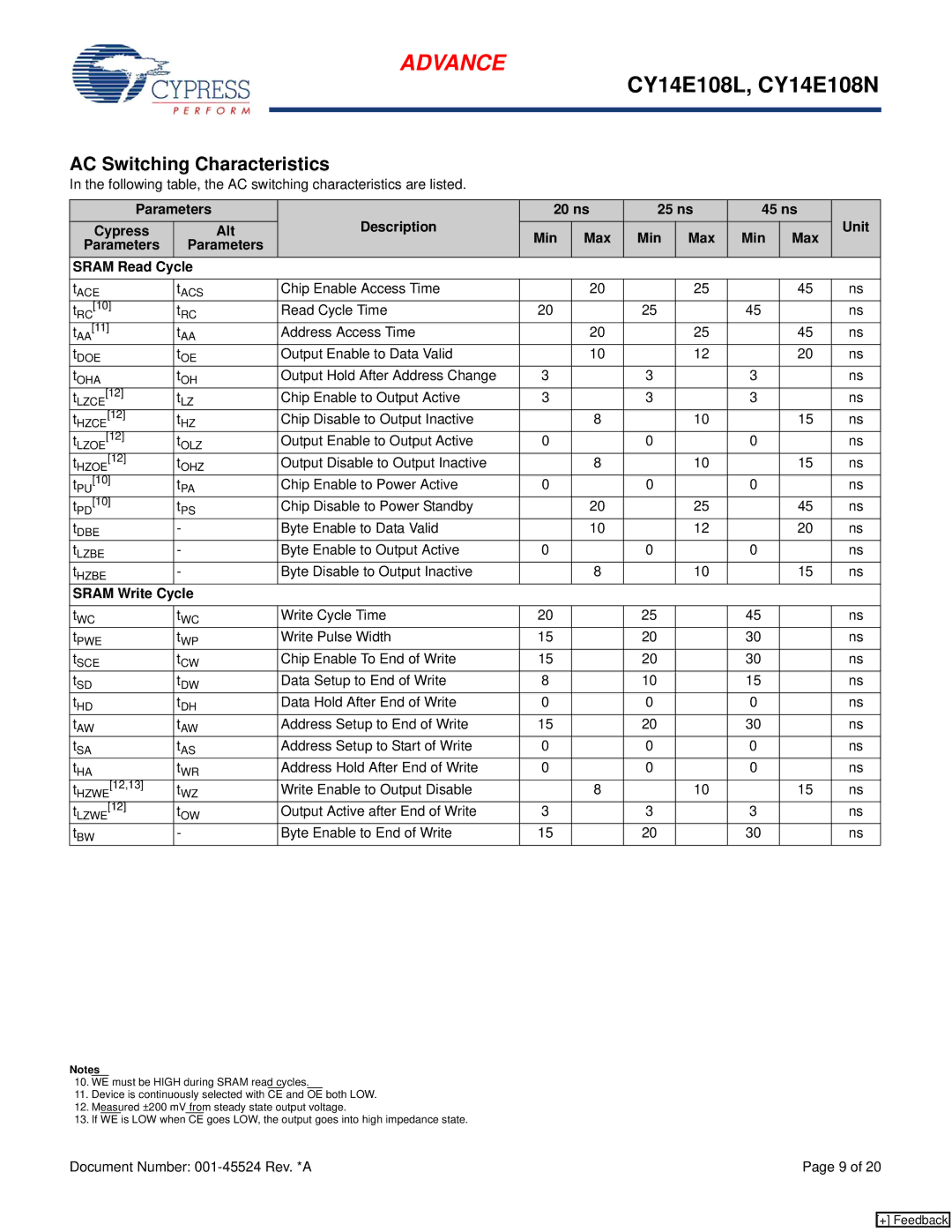
CY14E108N, CY14B102N specifications
Cypress Semiconductor, a leader in embedded memory solutions, offers a range of non-volatile memory products, among which the CY14B102N and CY14E108N stand out due to their advanced features and robust technology. Both devices are part of Cypress's NVSRAM (Non-Volatile Static Random Access Memory) family, combining the reliability of SRAM with the non-volatility of EEPROM.The CY14B102N is a 1 Megabit (128 Kilobyte) NVSRAM that utilizes a 2.5V to 3.6V power supply. It features a fast access time of 45 ns, making it suitable for high-speed applications. This device offers a unique advantage by providing data retention for up to 20 years without the need for battery backups, ensuring critical information remains intact even in power-off situations. The CY14B102N also incorporates write cycling endurance rated for over a million cycles, which is ideal for applications requiring frequent data updates.
On the other hand, the CY14E108N features 8 Megabits (1 Megabyte) of NVSRAM, operating at a power supply voltage range of 3.0V to 3.6V. It is designed for higher density applications, while still achieving fast access times of 45 ns. The data retention performance of the CY14E108N similarly allows for up to 20 years of stable data storage under power-off conditions. The device supports a wide range of serial interface protocols, further enhancing its integration capabilities with various microcontrollers and systems.
Both devices implement Cypress's proprietary technology that enables nearly instant data access without requiring a dedicated battery. This makes them suitable for applications in automotive, industrial, consumer, and telecommunications sectors, where maintaining data integrity is critical. The combination of high speed, endurance, and data retention makes the CY14B102N and CY14E108N ideal for systems requiring fast and reliable data storage.
Furthermore, the compatibility of these devices with standard SRAM interfaces ensures seamless integration into existing designs, minimizing design complexity. With their advanced features and reliable performance, Cypress's NVSRAM products provide a compelling solution for high-performance non-volatile memory needs in modern electronic systems.

