PRELIMINARY | CY14B108K, CY14B108M |
|
8 Mbit (1024K x 8/512K x 16) nvSRAM with Real Time Clock
Features
■20 ns, 25 ns, and 45 ns access times
■Internally organized as 1024K x 8 (CY14B108K) or 512K x 16 (CY14B108M)
■Hands off automatic STORE on power down with only a small capacitor
■STORE to QuantumTrap® nonvolatile elements is initiated by software, device pin, or AutoStore® on power down
■RECALL to SRAM initiated by software or power up
■High reliability
■Infinite Read, Write, and RECALL cycles
■200,000 STORE cycles to QuantumTrap
■20 year data retention
■Single 3V +20%,
■Data integrity of Cypress nvSRAM combined with full featured Real Time Clock (RTC)
■Watchdog timer
■Clock alarm with programmable interrupts
■Capacitor or battery backup for RTC
■Commercial and industrial temperatures
■44 and
■
Functional Description
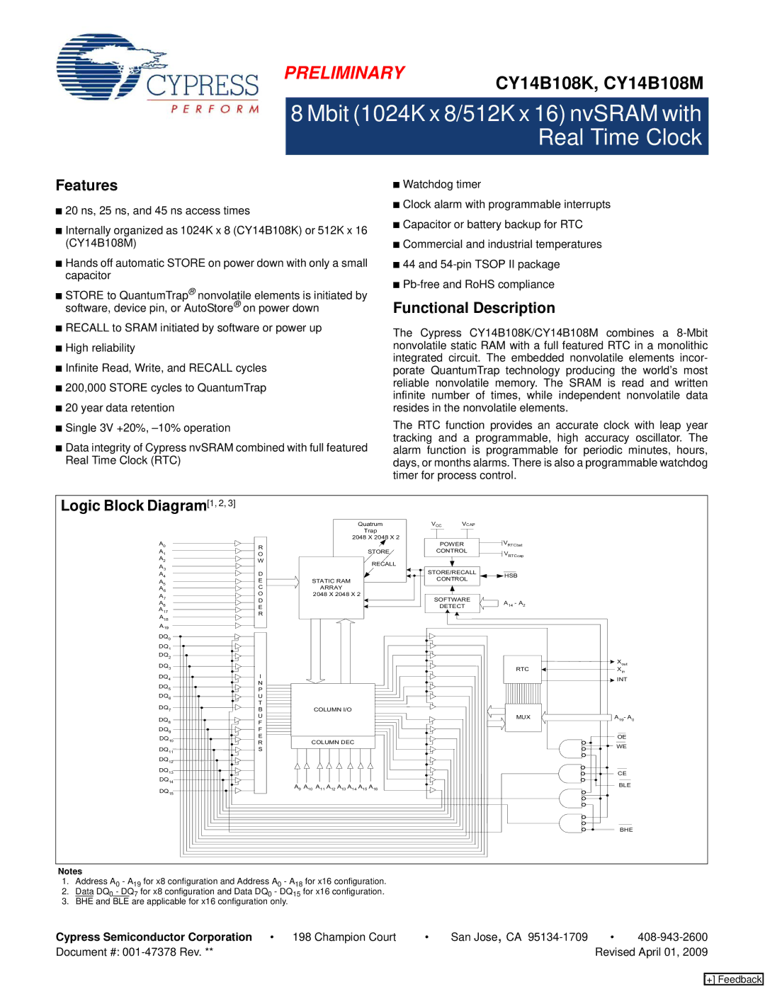
The Cypress CY14B108K/CY14B108M combines a
The RTC function provides an accurate clock with leap year tracking and a programmable, high accuracy oscillator. The alarm function is programmable for periodic minutes, hours, days, or months alarms. There is also a programmable watchdog timer for process control.
R O W
D E C O D E R
Quatrum | VCC | VCAP |
| |
Trap |
|
|
| |
2048 X 2048 X 2 | POWER | VRTCbat | ||
| ||||
STORE | CONTROL | VRTCcap | ||
|
|
| ||
RECALL |
|
|
| |
| STORE/RECALL | HSB | ||
STATIC RAM | CONTROL | |||
| ||||
ARRAY |
|
|
| |
2048 X 2048 X 2 | SOFTWARE |
| ||
| A14 - A2 | |||
| DETECT | |||
|
| |||
DQ3
DQ4
DQ5 DQ6
DQ7
DQ8 DQ9 DQ10
DQ11
DQ12
DQ13 DQ14
DQ15
I
N P U T B U F F E R S
COLUMN I/O
COLUMN DEC
A9 A10 A11 A12 A13 A14 A15 A16
| Xout |
RTC | Xin |
| INT |
MUX | A19- A0 |
| OE |
| WE |
| CE |
| BLE |
| BHE |
Notes |
|
|
|
|
| ||
1. | Address A0 - A19 for x8 configuration and Address A0 - A18 for x16 configuration. |
|
|
|
| ||
2. | Data DQ0 | - DQ7 for x8 configuration and Data DQ0 | - DQ15 for x16 configuration. |
|
|
|
|
3. | BHE and | BLE are applicable for x16 configuration only. |
|
|
|
| |
Cypress Semiconductor Corporation • | 198 Champion Court | • | San Jose, CA | • | |||
Document #: |
|
|
| Revised April 01, 2009 | |||
[+] Feedback