|
|
| PRELIMINARY | CY14B108K, CY14B108M | |||||||
|
|
|
|
| |||||||
|
|
|
|
|
|
|
|
|
|
|
|
|
|
|
|
|
|
|
|
|
|
| |
Data Retention and Endurance |
|
|
|
|
|
|
|
| |||
|
|
|
|
|
|
|
|
|
|
|
|
Parameter |
|
| Description | Min |
|
| Unit |
|
|
| |
DATAR | Data Retention | 20 |
|
| Years |
|
|
| |||
NVC | Nonvolatile STORE Operations | 200 |
|
| K |
|
|
| |||
Capacitance |
|
|
|
|
|
|
|
|
|
|
|
In the following table, the capacitance parameters are listed. [13] |
|
|
|
|
|
|
| ||||
Parameter |
|
| Description | Test Conditions |
| Max |
| Unit |
|
| |
CIN | Input Capacitance | TA = 25°C, f = 1 MHz, |
| 14 |
|
| pF |
|
| ||
|
| VCC = 0 to 3.0V |
|
|
|
|
|
| |||
COUT | Output Capacitance |
| 14 |
|
| pF |
|
| |||
Thermal Resistance |
|
|
|
|
|
|
|
| |||
In the following table, the thermal resistance parameters are listed.[13] |
|
|
|
|
|
|
| ||||
Parameter |
|
| Description | Test Conditions |
| 44 TSOP II | 54 TSOP II | Unit |
|
| |
ΘJA | Thermal Resistance | Test conditions follow standard test | 31.11 | 30.73 | °C/W |
|
| ||||
| (Junction to Ambient) | methods and procedures for |
|
|
|
|
|
|
| ||
|
|
|
| measuring thermal impedance, in |
|
|
|
|
|
| |
ΘJC | Thermal Resistance | 5.56 | 6.08 | °C/W |
|
| |||||
accordance with EIA/JESD51. |
| ||||||||||
| (Junction to Case) |
|
|
|
|
|
|
|
| ||
|
|
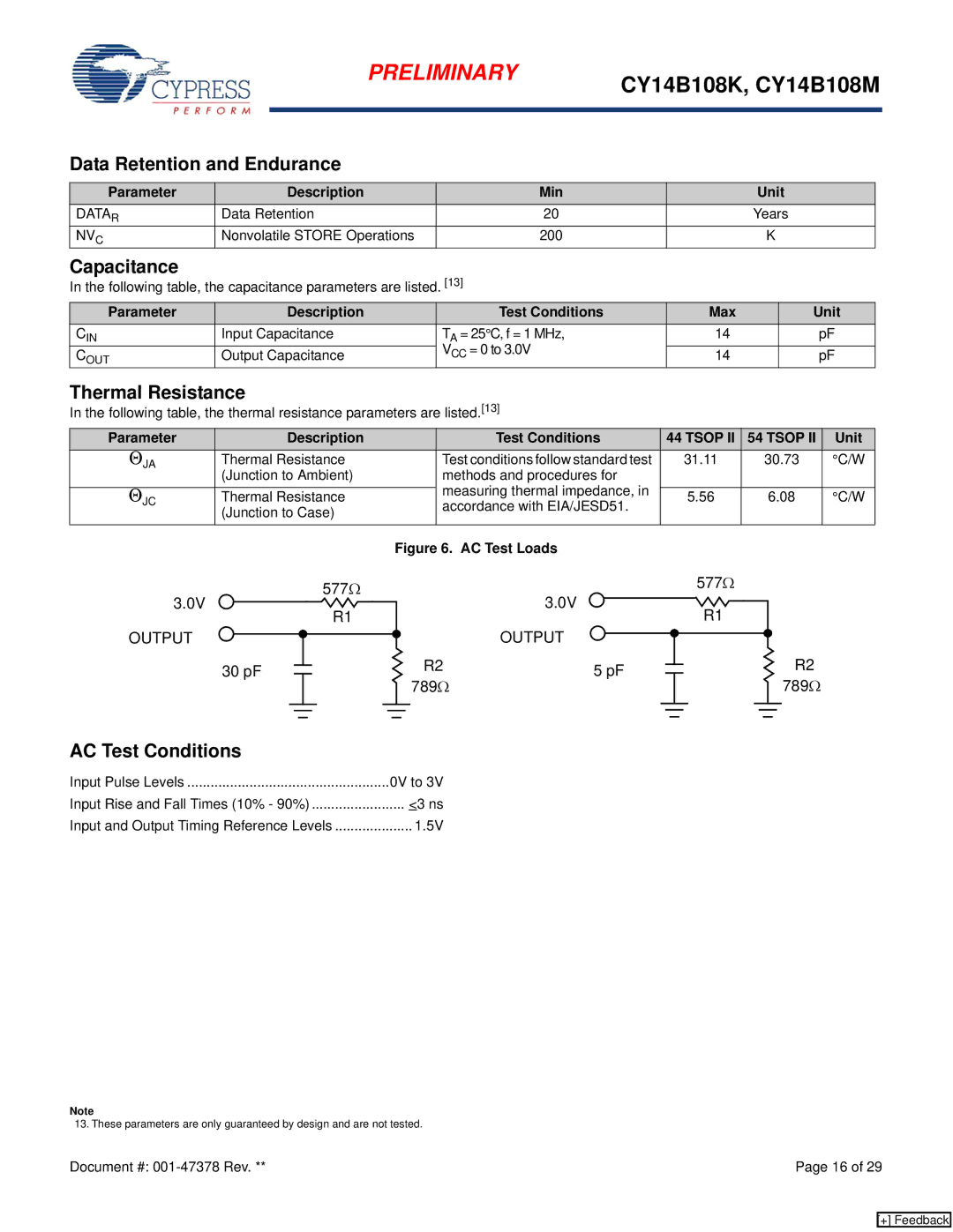
| Figure 6. AC Test Loads |
|
|
|
|
|
|
| |
3.0V | 577Ω | 3.0V | |
R1 | |||
| OUTPUT | ||
OUTPUT |
| ||
30 pF | R2 | 5 pF | |
| 789Ω |
|
577Ω
R1
![]() R2
R2 ![]() 789Ω
789Ω
AC Test Conditions
Input Pulse Levels | 0V to 3V |
Input Rise and Fall Times (10% - 90%) | <3 ns |
Input and Output Timing Reference Levels | 1.5V |
Note
13. These parameters are only guaranteed by design and are not tested.
Document #: | Page 16 of 29 |
[+] Feedback