|
|
|
|
|
|
|
|
|
|
|
|
|
|
|
|
|
|
|
|
|
| PRELIMINARY | CY14B108K, CY14B108M | ||
|
|
|
|
|
|
|
|
|
|
|
|
|
|
|
|
|
|
|
|
|
|
| |||
|
|
|
|
|
|
|
|
|
|
|
|
|
|
|
|
|
|
|
|
|
|
| |||
|
|
|
|
|
|
|
|
|
|
|
|
|
|
|
|
|
|
|
|
|
| ||||
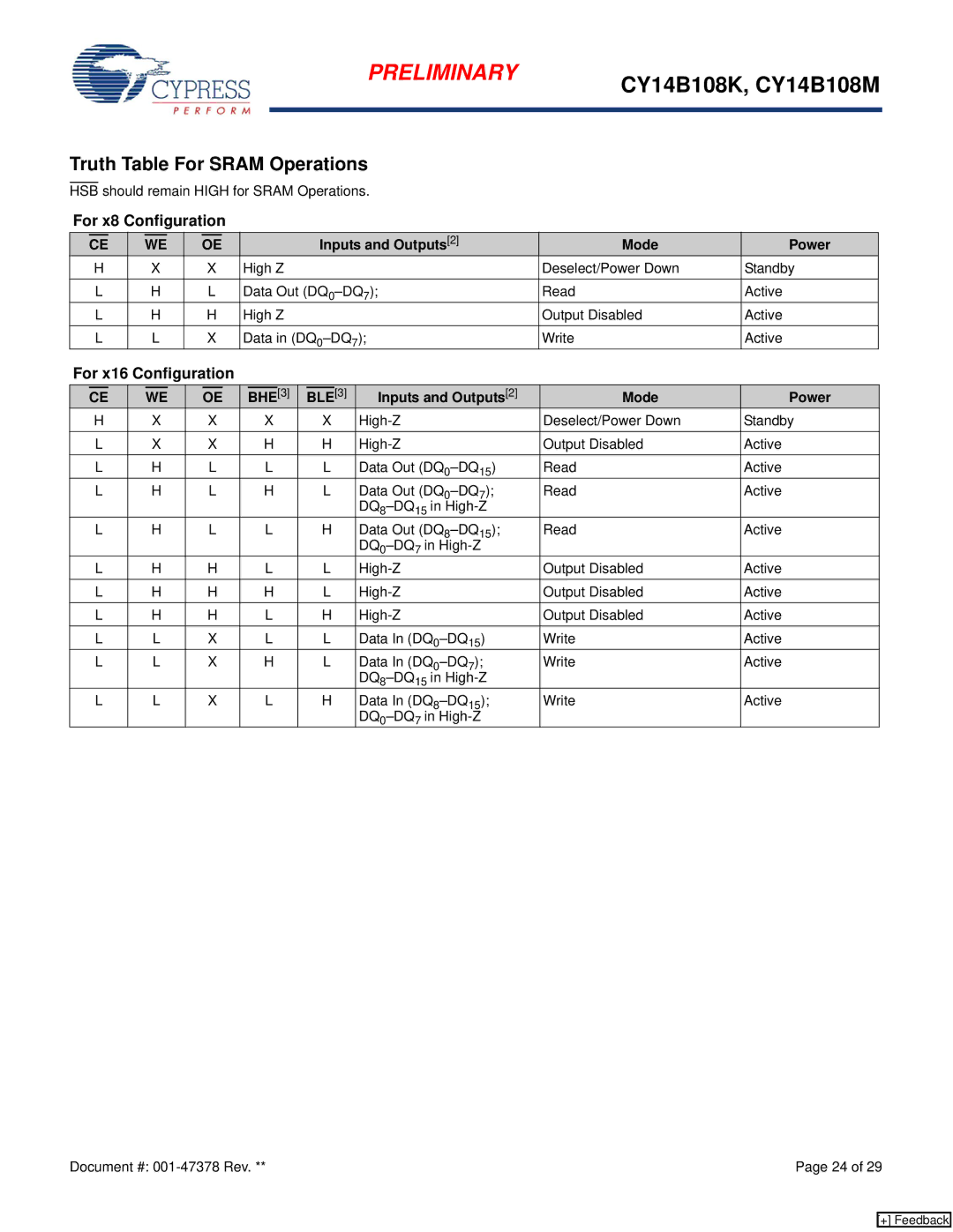
Truth Table For SRAM Operations |
|
|
| ||||||||||||||||||||||
|
| should remain HIGH for SRAM Operations. |
|
|
| ||||||||||||||||||||
HSB |
|
|
| ||||||||||||||||||||||
For x8 Configuration |
|
|
|
|
|
|
|
|
|
|
|
| |||||||||||||
| CE |
|
| WE |
|
|
| OE |
|
|
|
|
|
|
|
| Inputs and Outputs[2] | Mode | Power |
| |||||
| H |
|
|
| X |
|
| X | High Z |
|
|
| Deselect/Power Down | Standby |
| ||||||||||
| L |
|
|
| H |
|
| L | Data Out | Read | Active |
| |||||||||||||
| L |
|
|
| H |
|
| H | High Z |
|
|
| Output Disabled | Active |
| ||||||||||
| L |
|
|
| L |
|
| X | Data in | Write | Active |
| |||||||||||||
For x16 Configuration |
|
|
|
|
|
|
|
|
|
|
|
| |||||||||||||
| CE |
|
|
| WE |
|
|
| OE |
|
| BHE | [3] |
| BLE | [3] | Inputs and Outputs[2] | Mode | Power |
| |||||
| H |
|
|
| X |
|
| X |
| X |
| X | Deselect/Power Down | Standby |
| ||||||||||
| L |
|
|
| X |
|
| X |
| H |
| H | Output Disabled | Active |
| ||||||||||
| L |
|
|
| H |
|
| L |
| L |
| L | Data Out | Read | Active |
| |||||||||
| L |
|
|
| H |
|
| L |
| H |
| L | Data Out | Read | Active |
| |||||||||
|
|
|
|
|
|
|
|
|
|
|
|
|
|
|
|
|
|
|
|
|
|
|
|
| |
| L |
|
|
| H |
|
| L |
| L |
| H | Data Out | Read | Active |
| |||||||||
|
|
|
|
|
|
|
|
|
|
|
|
|
|
|
|
|
|
|
|
|
|
|
|
| |
| L |
|
|
| H |
|
| H |
| L |
| L | Output Disabled | Active |
| ||||||||||
| L |
|
|
| H |
|
| H |
| H |
| L | Output Disabled | Active |
| ||||||||||
| L |
|
|
| H |
|
| H |
| L |
| H | Output Disabled | Active |
| ||||||||||
| L |
|
|
| L |
|
| X |
| L |
| L | Data In | Write | Active |
| |||||||||
| L |
|
|
| L |
|
| X |
| H |
| L | Data In | Write | Active |
| |||||||||
|
|
|
|
|
|
|
|
|
|
|
|
|
|
|
|
|
|
|
|
|
|
|
|
| |
| L |
|
|
| L |
|
| X |
| L |
| H | Data In | Write | Active |
| |||||||||
|
|
|
|
|
|
|
|
|
|
|
|
|
|
|
|
|
|
|
|
|
|
|
|
| |
Document #: | Page 24 of 29 |
[+] Feedback