CY24272
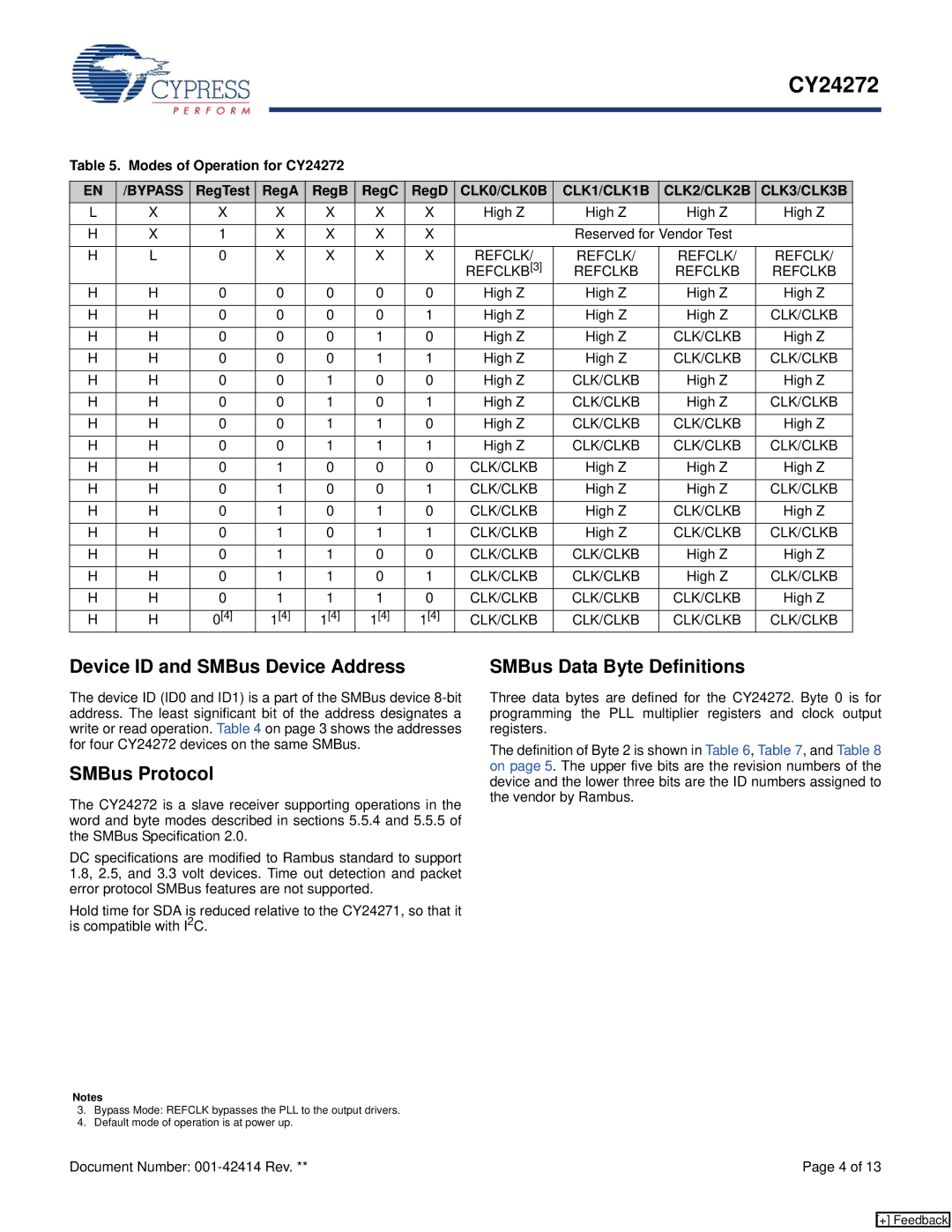
Table 5. Modes of Operation for CY24272
EN | /BYPASS | RegTest | RegA | RegB | RegC | RegD | CLK0/CLK0B | CLK1/CLK1B | CLK2/CLK2B | CLK3/CLK3B |
L | X | X | X | X | X | X | High Z | High Z | High Z | High Z |
|
|
|
|
|
|
|
|
|
|
|
H | X | 1 | X | X | X | X |
| Reserved for | Vendor Test |
|
|
|
|
|
|
|
|
|
|
|
|
H | L | 0 | X | X | X | X | REFCLK/ | REFCLK/ | REFCLK/ | REFCLK/ |
|
|
|
|
|
|
| REFCLKB[3] | REFCLKB | REFCLKB | REFCLKB |
H | H | 0 | 0 | 0 | 0 | 0 | High Z | High Z | High Z | High Z |
|
|
|
|
|
|
|
|
|
|
|
H | H | 0 | 0 | 0 | 0 | 1 | High Z | High Z | High Z | CLK/CLKB |
|
|
|
|
|
|
|
|
|
|
|
H | H | 0 | 0 | 0 | 1 | 0 | High Z | High Z | CLK/CLKB | High Z |
|
|
|
|
|
|
|
|
|
|
|
H | H | 0 | 0 | 0 | 1 | 1 | High Z | High Z | CLK/CLKB | CLK/CLKB |
|
|
|
|
|
|
|
|
|
|
|
H | H | 0 | 0 | 1 | 0 | 0 | High Z | CLK/CLKB | High Z | High Z |
|
|
|
|
|
|
|
|
|
|
|
H | H | 0 | 0 | 1 | 0 | 1 | High Z | CLK/CLKB | High Z | CLK/CLKB |
|
|
|
|
|
|
|
|
|
|
|
H | H | 0 | 0 | 1 | 1 | 0 | High Z | CLK/CLKB | CLK/CLKB | High Z |
|
|
|
|
|
|
|
|
|
|
|
H | H | 0 | 0 | 1 | 1 | 1 | High Z | CLK/CLKB | CLK/CLKB | CLK/CLKB |
|
|
|
|
|
|
|
|
|
|
|
H | H | 0 | 1 | 0 | 0 | 0 | CLK/CLKB | High Z | High Z | High Z |
|
|
|
|
|
|
|
|
|
|
|
H | H | 0 | 1 | 0 | 0 | 1 | CLK/CLKB | High Z | High Z | CLK/CLKB |
|
|
|
|
|
|
|
|
|
|
|
H | H | 0 | 1 | 0 | 1 | 0 | CLK/CLKB | High Z | CLK/CLKB | High Z |
|
|
|
|
|
|
|
|
|
|
|
H | H | 0 | 1 | 0 | 1 | 1 | CLK/CLKB | High Z | CLK/CLKB | CLK/CLKB |
|
|
|
|
|
|
|
|
|
|
|
H | H | 0 | 1 | 1 | 0 | 0 | CLK/CLKB | CLK/CLKB | High Z | High Z |
|
|
|
|
|
|
|
|
|
|
|
H | H | 0 | 1 | 1 | 0 | 1 | CLK/CLKB | CLK/CLKB | High Z | CLK/CLKB |
|
|
|
|
|
|
|
|
|
|
|
H | H | 0 | 1 | 1 | 1 | 0 | CLK/CLKB | CLK/CLKB | CLK/CLKB | High Z |
|
|
|
|
|
|
|
|
|
|
|
H | H | 0[4] | 1[4] | 1[4] | 1[4] | 1[4] | CLK/CLKB | CLK/CLKB | CLK/CLKB | CLK/CLKB |
Device ID and SMBus Device Address
The device ID (ID0 and ID1) is a part of the SMBus device
SMBus Protocol
The CY24272 is a slave receiver supporting operations in the word and byte modes described in sections 5.5.4 and 5.5.5 of the SMBus Specification 2.0.
DC specifications are modified to Rambus standard to support 1.8, 2.5, and 3.3 volt devices. Time out detection and packet error protocol SMBus features are not supported.
Hold time for SDA is reduced relative to the CY24271, so that it is compatible with I2C.
SMBus Data Byte Definitions
Three data bytes are defined for the CY24272. Byte 0 is for programming the PLL multiplier registers and clock output registers.
The definition of Byte 2 is shown in Table 6, Table 7, and Table 8 on page 5. The upper five bits are the revision numbers of the device and the lower three bits are the ID numbers assigned to the vendor by Rambus.
Notes
3.Bypass Mode: REFCLK bypasses the PLL to the output drivers.
4.Default mode of operation is at power up.
Document Number: | Page 4 of 13 |
[+] Feedback
