CY24272
Rambus→ XDR™ Clock Generator with Zero SDA Hold Time
Features
■Meets Rambus→ Extended Data Rate (XDR™) clocking requirements
■25 ps typical
❐
■100 or 133 MHz differential clock input
■
■Quad (open drain) differential output drivers
■Supports frequency multipliers: 3, 4, 5, 6, 9/2 and 15/4
■Spread Aware™
■2.5V operation
■
Table 1. Device Comparison
CY24271 | CY24272 |
SDA hold time = 300 ns | SDA hold time = 0 ns |
(SMBus compliant) | (I2C compliant) |
RRC = 200Ω typical | RRC = 295Ω minimum |
(Rambus standard drive) | (Reduced output drive) |
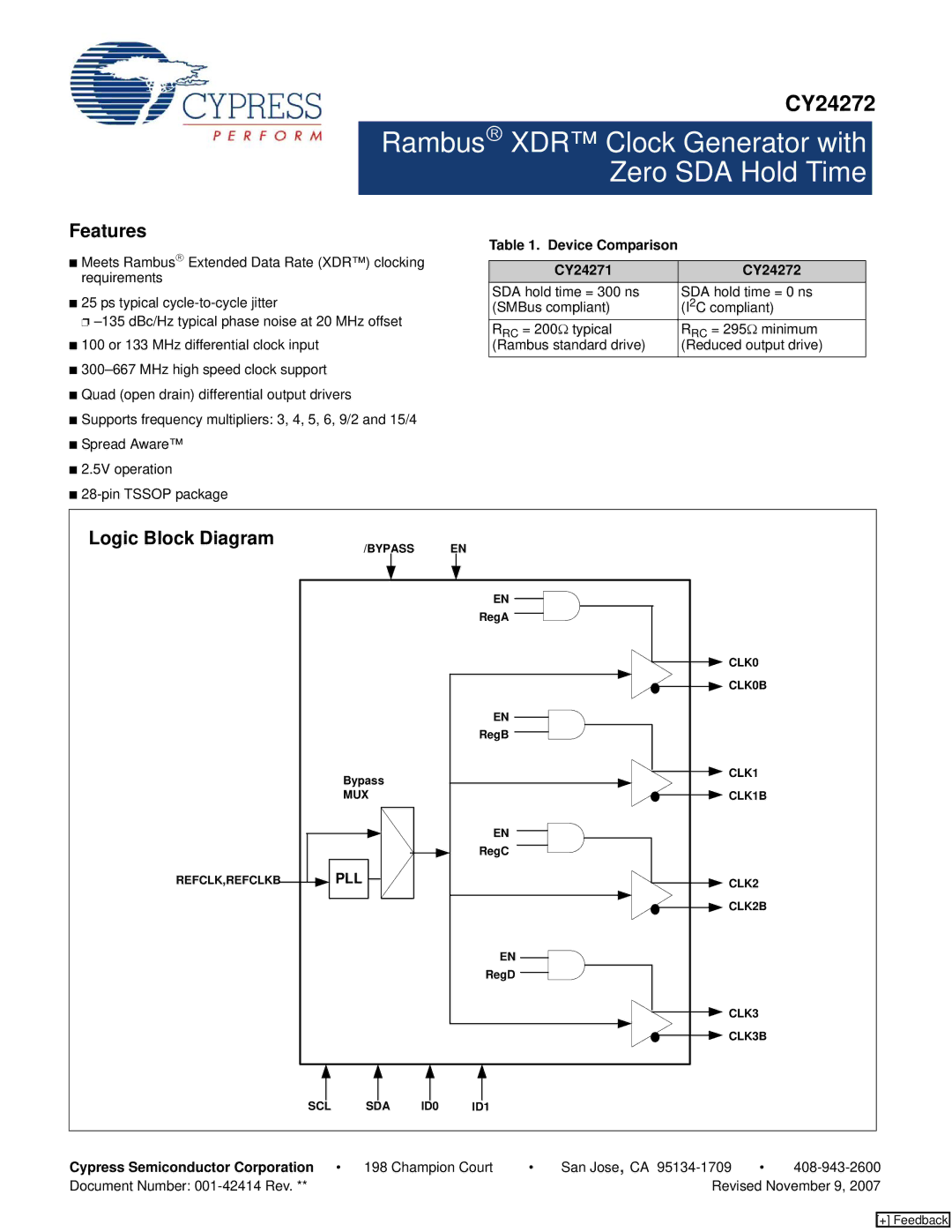
Logic Block Diagram
REFCLK,REFCLKB
| /BYPASS |
| EN |
|
|
| EN |
|
|
| RegA |
|
|
| CLK0 |
|
|
| CLK0B |
|
|
| EN |
|
|
| RegB |
| Bypass |
| CLK1 |
|
|
| |
| MUX |
| CLK1B |
|
|
| EN |
|
|
| RegC |
| PLL |
| CLK2 |
|
|
| CLK2B |
|
|
| EN |
|
|
| RegD |
|
|
| CLK3 |
|
|
| CLK3B |
SCL | SDA | ID0 | ID1 |
Cypress Semiconductor Corporation • 198 Champion Court | • | San Jose, CA | • | |
Document Number: |
| Revised November 9, 2007 | ||
[+] Feedback