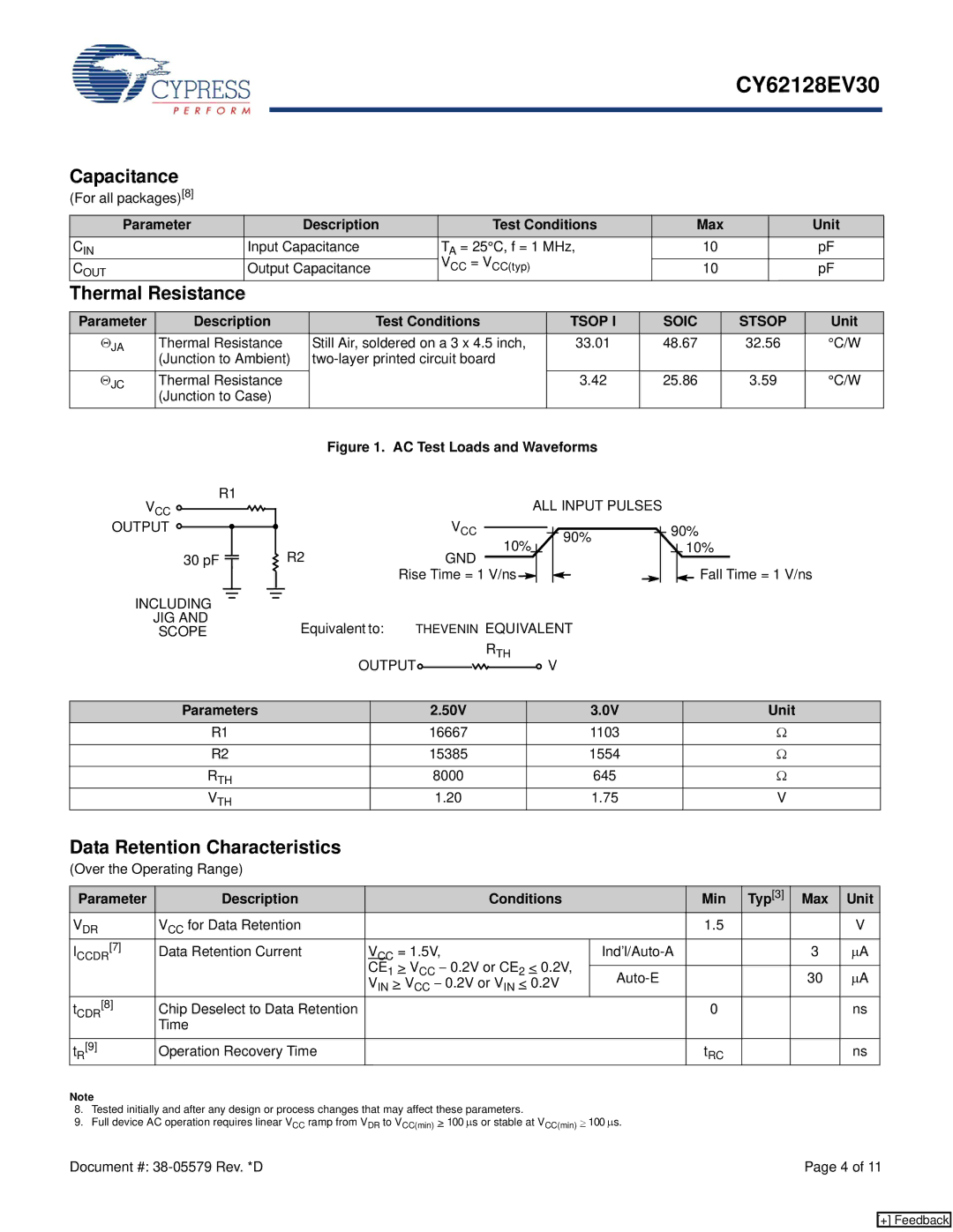
CY62128EV30 specifications
The Cypress CY62128EV30 is a high-performance CMOS SRAM (Static Random Access Memory) device that is widely used in various applications due to its advanced technology and robust characteristics. As a 1-megabit SRAM, it features a 128K x 8 bit organization, providing ample storage capacity for a range of modern electronic devices.One of the key features of the CY62128EV30 is its fast access time, with read cycle times available in the range of 30 to 70 nanoseconds. This rapid access speed is essential for applications that require quick data retrieval, making it ideal for use in high-speed computing environments. Additionally, it boasts a low power consumption profile, typically operating at 2.7V to 3.6V, allowing it to meet the demands of power-sensitive applications while ensuring energy efficiency.
In terms of technology, the CY62128EV30 utilizes advanced CMOS processes that contribute to its smaller footprint and higher reliability. The device includes a full asynchronous design, allowing for simple interface with other digital logic components without the need for complicated timing signals. This characteristic simplifies the overall system design, making it easier to integrate into various circuit configurations.
The CY62128EV30 also offers a wide operational temperature range, typically from -40°C to +85°C, which enhances its suitability for use in harsh environments or industrial applications. This durability ensures that the device maintains its performance specifications even under extreme conditions.
Moreover, the device features a tri-state output and supports both read and write operations with a single chip select pin, enhancing its versatility in multiple configurations. The ability to easily interface in a variety of systems makes it a preferred choice for designs requiring flexible memory solutions.
The CY62128EV30 is compatible with standard microprocessor architectures, making it ideal for use in applications such as networking equipment, telecommunications, consumer electronics, and embedded systems. Its reliability, combined with efficient power management and fast access speeds, make it a trusted solution in the fast-evolving technology landscape.
In conclusion, the Cypress CY62128EV30 stands out due to its combination of speed, power efficiency, and operational versatility, making it a valuable component in contemporary electronic design. Its cutting-edge technology and features cater to the growing demands of high-performance applications across various industries.

