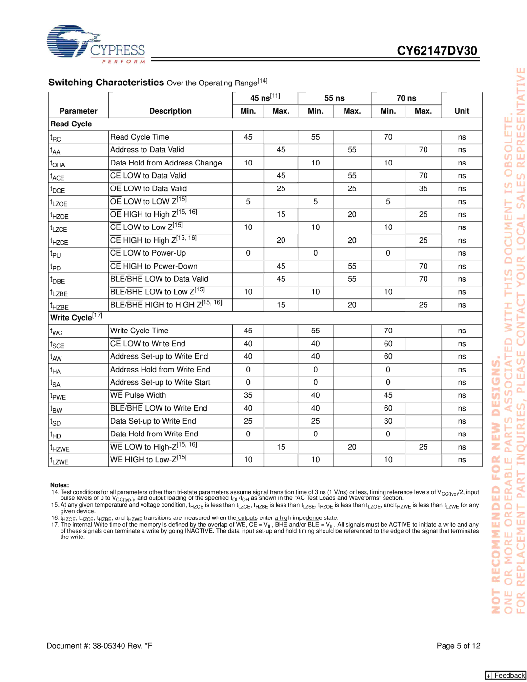
CY62147DV30
Switching Characteristics Over the Operating Range[14]
|
|
|
|
|
|
|
|
| 45 ns[11] |
| 55 ns |
| 70 ns |
| |||
Parameter |
|
|
|
|
|
|
| Description | Min. | Max. | Min. |
| Max. | Min. |
| Max. | Unit |
|
|
|
|
|
|
|
|
|
|
|
|
|
|
|
|
|
|
Read Cycle |
|
|
|
|
|
|
|
|
|
|
|
|
|
|
|
| |
|
|
|
|
|
|
|
|
|
|
| |||||||
tRC |
| Read Cycle Time | 45 |
| 55 |
|
| 70 |
|
| ns | ||||||
tAA |
| Address to Data Valid |
| 45 |
|
| 55 |
|
| 70 | ns | ||||||
tOHA |
| Data Hold from Address Change | 10 |
| 10 |
|
| 10 |
|
| ns | ||||||
tACE |
|
|
|
| LOW to Data Valid |
| 45 |
|
| 55 |
|
| 70 | ns | |||
CE |
|
|
| ||||||||||||||
tDOE |
|
|
|
| LOW to Data Valid |
| 25 |
|
| 25 |
|
| 35 | ns | |||
OE |
|
|
| ||||||||||||||
tLZOE |
|
|
|
| LOW to LOW Z[15] | 5 |
| 5 |
|
| 5 |
|
| ns | |||
OE |
|
|
|
|
| ||||||||||||
tHZOE |
|
|
|
| HIGH to High Z[15, 16] |
| 15 |
|
| 20 |
|
| 25 | ns | |||
OE |
|
|
| ||||||||||||||
tLZCE |
|
|
| LOW to Low Z[15] | 10 |
| 10 |
|
| 10 |
|
| ns | ||||
CE |
|
|
|
|
| ||||||||||||
tHZCE |
|
|
| HIGH to High Z[15, 16] |
| 20 |
|
| 20 |
|
| 25 | ns | ||||
CE |
|
|
| ||||||||||||||
tPU |
|
|
| LOW to | 0 |
| 0 |
|
| 0 |
|
| ns | ||||
CE |
|
|
|
|
| ||||||||||||
tPD |
|
|
| HIGH to |
| 45 |
|
| 55 |
|
| 70 | ns | ||||
CE |
|
|
| ||||||||||||||
tDBE |
|
|
|
|
|
|
|
|
| 45 |
|
| 55 |
|
| 70 | ns |
BLE/BHE LOW to Data Valid |
|
|
| ||||||||||||||
t |
|
|
|
|
|
|
|
| 10 |
| 10 |
|
| 10 |
|
| ns |
BLE/BHE LOW to Low Z[15] |
|
|
|
|
| ||||||||||||
LZBE |
|
|
|
|
|
|
|
|
|
|
|
|
|
|
|
|
|
t |
|
|
|
|
|
|
|
|
| 15 |
|
| 20 |
|
| 25 | ns |
BLE/BHE HIGH to HIGH Z[15, 16] |
|
|
| ||||||||||||||
HZBE |
|
|
|
|
|
|
|
|
|
|
|
|
|
|
|
|
|
Write Cycle[17] |
|
|
|
|
|
|
|
|
|
|
|
|
|
|
|
|
|
tWC |
| Write Cycle Time | 45 |
| 55 |
|
| 70 |
|
| ns | ||||||
tSCE |
|
|
| LOW to Write End | 40 |
| 40 |
|
| 60 |
|
| ns | ||||
CE |
|
|
|
|
| ||||||||||||
tAW |
| Address | 40 |
| 40 |
|
| 60 |
|
| ns | ||||||
tHA |
| Address Hold from Write End | 0 |
| 0 |
|
| 0 |
|
| ns | ||||||
tSA |
| Address | 0 |
| 0 |
|
| 0 |
|
| ns | ||||||
tPWE |
|
|
|
| Pulse Width | 35 |
| 40 |
|
| 45 |
|
| ns | |||
WE |
|
|
|
|
| ||||||||||||
tBW |
|
|
|
|
|
|
|
| 40 |
| 40 |
|
| 60 |
|
| ns |
BLE/BHE LOW to Write End |
|
|
|
|
| ||||||||||||
tSD |
| Data | 25 |
| 25 |
|
| 30 |
|
| ns | ||||||
tHD |
| Data Hold from Write End | 0 |
| 0 |
|
| 0 |
|
| ns | ||||||
tHZWE |
|
|
|
| LOW to |
| 15 |
|
| 20 |
|
| 25 | ns | |||
WE |
|
|
| ||||||||||||||
tLZWE |
|
|
|
| HIGH to | 10 |
| 10 |
|
| 10 |
|
| ns | |||
WE |
|
|
|
|
| ||||||||||||
Notes:
14.Test conditions for all parameters other than
15.At any given temperature and voltage condition, tHZCE is less than tLZCE, tHZBE is less than tLZBE, tHZOE is less than tLZOE, and tHZWE is less than tLZWE for any given device.
16.tHZOE, tHZCE, tHZBE, and tHZWE transitions are measured when the outputs enter a high impedence state.
17.The internal Write time of the memory is defined by the overlap of WE, CE = VIL, BHE and/or BLE = VIL. All signals must be ACTIVE to initiate a write and any of these signals can terminate a write by going INACTIVE. The data input
Document #: | Page 5 of 12 |
[+] Feedback