CY62167E MoBL®
Switching Waveforms (continued)
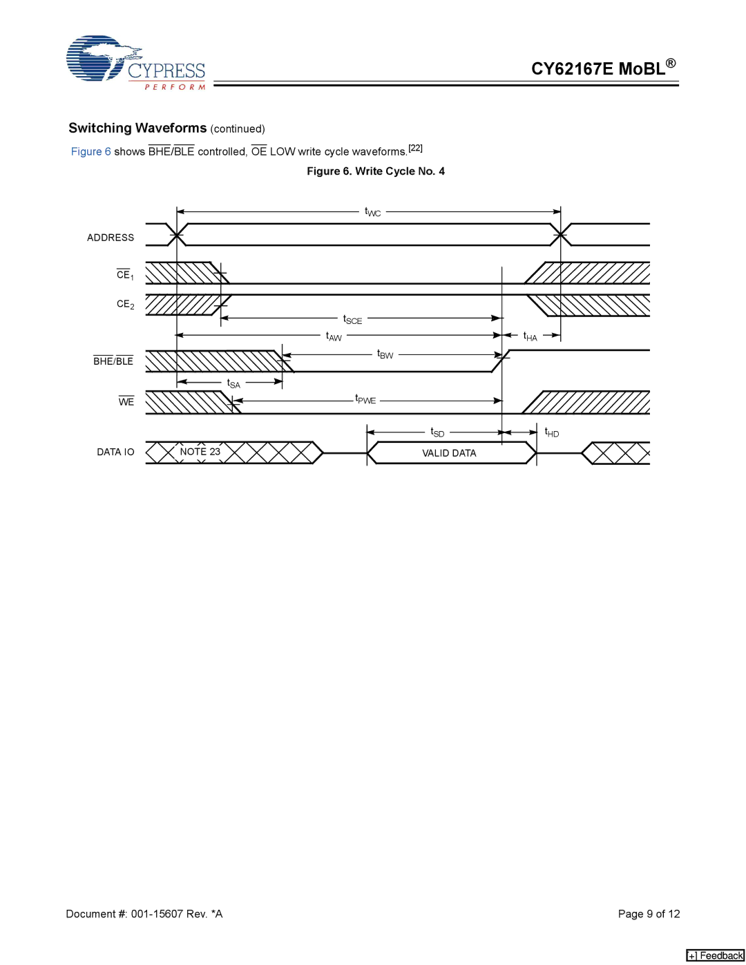
Figure 6 shows BHE/BLE controlled, OE LOW write cycle waveforms.[22]
Figure 6. Write Cycle No. 4
|
| tWC |
|
ADDRESS |
|
|
|
CE1 |
|
|
|
CE2 |
| tSCE |
|
|
|
| |
| tAW |
| tHA |
BHE/BLE |
| tBW |
|
|
|
| |
| tSA |
|
|
WE |
| tPWE |
|
|
| tSD | tHD |
DATA IO | NOTE 23 | VALID DATA |
|
Document #: | Page 9 of 12 |
[+] Feedback