CY62167E MoBL®
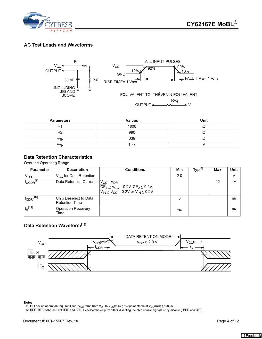
AC Test Loads and Waveforms
R1
VCC ![]()
OUTPUT ![]()
30 pF ![]()
INCLUDING
JIG AND
SCOPE
| VCC |
|
|
|
|
|
|
|
|
| ALL INPUT PULSES | |||||||||||
|
|
|
|
|
|
|
|
|
|
|
|
|
|
|
|
| 90% |
| ||||
|
| 10% |
|
|
|
|
|
| 90% |
|
|
|
|
|
|
| 10% | |||||
|
|
|
|
|
|
|
|
|
|
|
|
|
|
|
|
|
| |||||
R2 | GND |
|
|
|
|
|
|
|
|
|
|
|
|
|
|
|
|
| FALL TIME= 1 V/ns | |||
|
|
|
|
|
|
|
|
|
|
|
|
|
|
|
|
| ||||||
RISE TIME= 1 V/ns |
|
|
|
|
|
|
|
|
|
|
|
|
|
|
| |||||||
|
|
|
|
|
|
|
|
|
|
|
|
|
|
|
|
|
| |||||
|
| EQUIVALENT TO: THÉVENIN EQUIVALENT | ||||||||||||||||||||
|
|
|
| OUTPUT |
| RTH | ||||||||||||||||
|
|
|
|
|
|
|
|
|
|
|
|
| V | |||||||||
|
|
|
|
|
|
|
|
|
|
|
|
| ||||||||||
Parameters | Values | Unit |
R1 | 1800 | Ω |
|
|
|
R2 | 990 | Ω |
|
|
|
RTH | 639 | Ω |
VTH | 1.77 | V |
Data Retention Characteristics
Over the Operating Range
Parameter | Description | Conditions | Min | Typ[4] | Max | Unit | |
VDR | VCC for Data Retention |
| 2.0 |
|
| V | |
ICCDR[9] | Data Retention Current | VCC= VDR |
|
|
| 12 | ∝A |
|
| CE1 > VCC – 0.2V, CE2 < 0.2V, |
|
|
|
|
|
|
| VIN > VCC – 0.2V or VIN < 0.2V |
|
|
|
|
|
tCDR[10] | Chip Deselect to Data |
|
| 0 |
|
| ns |
| Retention Time |
|
|
|
|
|
|
t [11] | Operation Recovery |
| t | RC |
|
| ns |
R | Time |
|
|
|
|
| |
|
|
|
|
|
|
| |
|
|
|
|
|
|
|
|
Data Retention Waveform[12]
VCC
CE1 or
BHE. BLE or CE2
|
|
|
|
|
|
|
| DATA RETENTION MODE |
|
|
|
|
|
|
|
|
|
|
|
|
|
|
|
|
|
|
|
|
|
|
|
|
|
|
|
|
|
|
|
|
|
|
|
|
|
|
|
| |
|
|
|
|
|
|
|
|
|
|
|
|
|
|
|
|
|
|
|
|
|
|
|
| |
|
|
|
|
|
|
|
|
|
|
|
|
| VCC(min) |
|
|
|
| |||||||
VCC(min) |
|
|
|
|
| VDR > 2.0 V |
|
|
|
|
|
|
|
|
| |||||||||
|
|
|
|
|
|
|
|
|
|
|
|
| ||||||||||||
| tCDR |
|
|
|
|
|
|
|
|
|
|
|
|
| tR |
|
|
|
|
|
|
|
| |
|
|
|
|
|
|
| ||||||||||||||||||
|
|
|
|
|
|
|
|
|
|
|
|
|
|
|
|
|
|
|
| |||||
|
|
|
|
|
|
|
|
|
|
|
|
|
|
|
|
|
|
|
|
|
|
|
|
|
|
|
|
|
|
|
|
|
|
|
|
|
|
|
|
|
|
|
|
|
|
|
|
|
|
|
|
|
|
|
|
|
|
|
|
|
|
|
|
|
|
|
|
|
|
|
|
|
|
|
|
|
|
|
|
|
|
|
|
|
|
|
|
|
|
|
|
|
|
|
|
|
|
|
|
|
|
|
|
|
|
|
|
|
|
|
|
|
|
|
|
|
|
|
|
|
|
|
|
|
|
|
|
|
|
|
|
|
|
|
|
|
|
|
|
|
|
|
|
|
|
|
|
|
|
|
|
|
|
|
|
|
|
|
|
|
|
|
|
|
|
|
|
|
|
|
|
|
|
|
Notes
11.Full device operation requires linear VCC ramp from VDR to VCC(min) > 100 ∝s or stable at VCC(min) > 100 ∝s.
12.BHE. BLE is the AND of BHE and BLE. Deselect the chip by either disabling the chip enable signals or by disabling BHE and BLE.
Document #: | Page 4 of 12 |
[+] Feedback