|
|
|
|
|
|
|
|
|
|
|
|
|
|
|
|
|
|
|
|
|
|
|
|
|
|
|
|
|
| CY7C1292DV18 | ||||||||
|
|
|
|
|
|
|
|
|
|
|
|
|
|
|
|
|
|
|
|
|
|
|
|
|
|
|
|
|
| CY7C1294DV18 | ||||||||
|
|
|
|
|
|
|
|
|
|
|
|
|
|
|
|
|
|
|
|
|
|
|
|
|
|
|
|
|
|
|
|
|
|
|
|
|
|
|
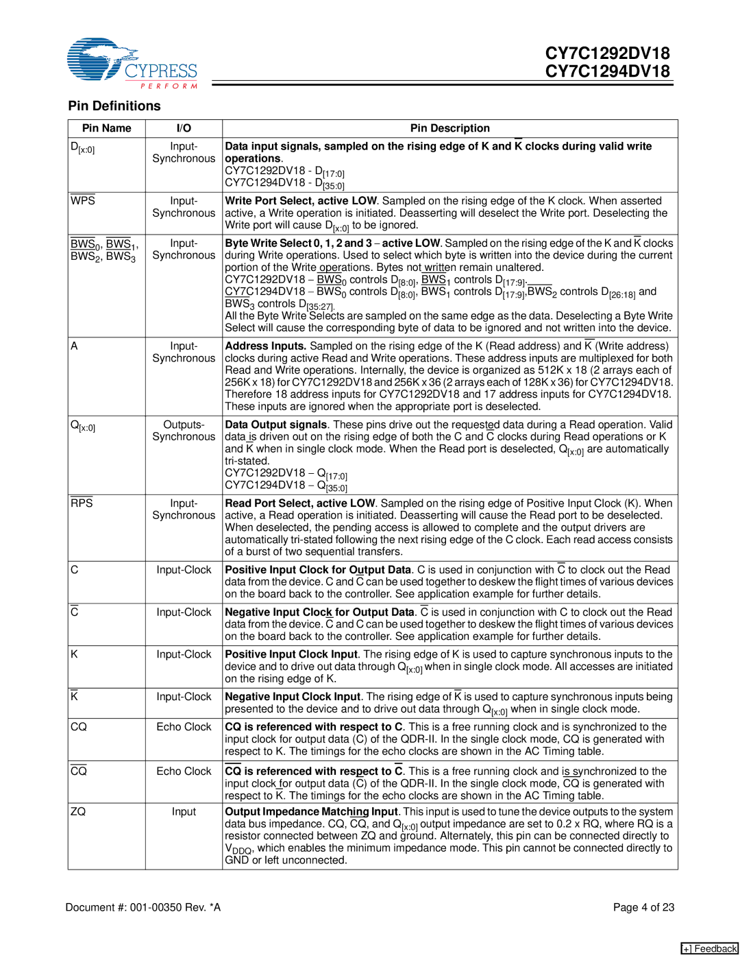
| Pin Definitions |
|
|
|
|
|
|
|
|
|
|
|
|
|
|
|
|
|
|
|
|
|
|
|
| |||||||||||||
|
|
|
|
|
|
|
|
|
|
|
|
|
|
|
| |||||||||||||||||||||||
|
|
|
| Pin Name | I/O |
|
|
|
|
|
|
|
|
| Pin Description | |||||||||||||||||||||||
|
|
|
|
|
|
|
|
|
|
|
|
|
|
|
|
|
|
|
|
|
|
|
|
|
|
|
|
|
|
|
| |||||||
|
| D[x:0] | Input- |
| Data input signals, sampled on the rising edge of K and | K | clocks during valid write | |||||||||||||||||||||||||||||||
|
|
|
|
|
|
|
|
|
|
| Synchronous |
| operations. |
|
|
|
|
|
|
|
|
|
|
|
|
|
|
|
|
|
| |||||||
|
|
|
|
|
|
|
|
|
|
|
|
|
|
| CY7C1292DV18 - D[17:0] |
|
|
|
|
|
|
|
|
|
|
|
|
|
|
|
|
|
| |||||
|
|
|
|
|
|
|
|
|
|
|
|
|
|
| CY7C1294DV18 - D[35:0] |
|
|
|
|
|
|
|
|
|
|
|
|
|
|
|
|
|
| |||||
|
|
|
|
|
|
|
|
|
| Input- |
| Write Port Select, active LOW. Sampled on the rising edge of the K clock. When asserted | ||||||||||||||||||||||||||
|
| WPS | ||||||||||||||||||||||||||||||||||||
|
|
|
|
|
|
|
|
|
|
| Synchronous |
| active, a Write operation is initiated. Deasserting will deselect the Write port. Deselecting the | |||||||||||||||||||||||||
|
|
|
|
|
|
|
|
|
|
|
|
|
|
| Write port will cause D[x:0] to be ignored. |
|
|
|
|
|
|
|
|
|
|
|
|
| ||||||||||
|
|
|
|
|
|
| 0, |
|
| 1, | Input- |
| Byte Write Select 0, 1, 2 and 3 − active LOW. Sampled on the rising edge of the K and |
| clocks | |||||||||||||||||||||||
|
| BWS | BWS | K | ||||||||||||||||||||||||||||||||||
|
| BWS2, BWS3 | Synchronous |
| during Write operations. Used to select which byte is written into the device during the current | |||||||||||||||||||||||||||||||||
|
|
|
|
|
|
|
|
|
|
|
|
|
|
| portion of the Write operations. Bytes not written remain unaltered. | |||||||||||||||||||||||
|
|
|
|
|
|
|
|
|
|
|
|
|
|
| CY7C1292DV18 − BWS0 | controls D[8:0], BWS1 | controls D[17:9]. |
|
|
|
|
|
| |||||||||||||||
|
|
|
|
|
|
|
|
|
|
|
|
|
|
| CY7C1294DV18 − BWS0 | controls D[8:0], BWS1 | controls D[17:9],BWS2 controls D[26:18] and | |||||||||||||||||||||
|
|
|
|
|
|
|
|
|
|
|
|
|
|
| BWS3 controls D[35:27]. |
|
|
|
|
|
|
|
|
|
|
|
|
|
|
|
|
|
| |||||
|
|
|
|
|
|
|
|
|
|
|
|
|
|
| All the Byte Write Selects are sampled on the same edge as the data. Deselecting a Byte Write | |||||||||||||||||||||||
|
|
|
|
|
|
|
|
|
|
|
|
|
|
| Select will cause the corresponding byte of data to be ignored and not written into the device. | |||||||||||||||||||||||
|
| A | Input- |
| Address Inputs. Sampled on the rising edge of the K (Read address) and |
| (Write address) | |||||||||||||||||||||||||||||||
|
| K | ||||||||||||||||||||||||||||||||||||
|
|
|
|
|
|
|
|
|
|
| Synchronous |
| clocks during active Read and Write operations. These address inputs are multiplexed for both | |||||||||||||||||||||||||
|
|
|
|
|
|
|
|
|
|
|
|
|
|
| Read and Write operations. Internally, the device is organized as 512K x 18 (2 arrays each of | |||||||||||||||||||||||
|
|
|
|
|
|
|
|
|
|
|
|
|
|
| 256K x 18) for CY7C1292DV18 and 256K x 36 (2 arrays each of 128K x 36) for CY7C1294DV18. | |||||||||||||||||||||||
|
|
|
|
|
|
|
|
|
|
|
|
|
|
| Therefore 18 address inputs for CY7C1292DV18 and 17 address inputs for CY7C1294DV18. | |||||||||||||||||||||||
|
|
|
|
|
|
|
|
|
|
|
|
|
|
| These inputs are ignored when the appropriate port is deselected. | |||||||||||||||||||||||
|
| Q[x:0] | Outputs- |
| Data Output signals. These pins drive out the requested data during a Read operation. Valid | |||||||||||||||||||||||||||||||||
|
|
|
|
|
|
|
|
|
|
| Synchronous |
| data is driven out on the rising edge of both the C and C clocks during Read operations or K | |||||||||||||||||||||||||
|
|
|
|
|
|
|
|
|
|
|
|
|
|
| and | K | when in single clock mode. When the Read port is deselected, Q[x:0] are automatically | |||||||||||||||||||||
|
|
|
|
|
|
|
|
|
|
|
|
|
|
|
|
|
|
|
|
|
|
|
|
|
|
|
|
|
|
|
|
|
| |||||
|
|
|
|
|
|
|
|
|
|
|
|
|
|
| CY7C1292DV18 − Q[17:0] |
|
|
|
|
|
|
|
|
|
|
|
|
|
|
|
|
|
| |||||
|
|
|
|
|
|
|
|
|
|
|
|
|
|
| CY7C1294DV18 − Q[35:0] |
|
|
|
|
|
|
|
|
|
|
|
|
|
|
|
|
|
| |||||
|
|
|
|
|
|
| Input- |
| Read Port Select, active LOW. Sampled on the rising edge of Positive Input Clock (K). When | |||||||||||||||||||||||||||||
|
| RPS | ||||||||||||||||||||||||||||||||||||
|
|
|
|
|
|
|
|
|
|
| Synchronous |
| active, a Read operation is initiated. Deasserting will cause the Read port to be deselected. | |||||||||||||||||||||||||
|
|
|
|
|
|
|
|
|
|
|
|
|
|
| When deselected, the pending access is allowed to complete and the output drivers are | |||||||||||||||||||||||
|
|
|
|
|
|
|
|
|
|
|
|
|
|
| automatically | |||||||||||||||||||||||
|
|
|
|
|
|
|
|
|
|
|
|
|
|
| of a burst of two sequential transfers. |
|
|
|
|
|
|
|
|
|
|
|
|
| ||||||||||
|
| C |
| Positive Input Clock for Output Data. C is used in conjunction with |
| to clock out the Read | ||||||||||||||||||||||||||||||||
|
| C | ||||||||||||||||||||||||||||||||||||
|
|
|
|
|
|
|
|
|
|
|
|
|
|
| data from the device. C and C can be used together to deskew the flight times of various devices | |||||||||||||||||||||||
|
|
|
|
|
|
|
|
|
|
|
|
|
|
| on the board back to the controller. See application example for further details. | |||||||||||||||||||||||
|
|
|
|
|
|
| Negative Input Clock for Output Data. |
| is used in conjunction with C to clock out the Read | |||||||||||||||||||||||||||||
|
| C | C | |||||||||||||||||||||||||||||||||||
|
|
|
|
|
|
|
|
|
|
|
|
|
|
| data from the device. C and C can be used together to deskew the flight times of various devices | |||||||||||||||||||||||
|
|
|
|
|
|
|
|
|
|
|
|
|
|
| on the board back to the controller. See application example for further details. | |||||||||||||||||||||||
|
| K |
| Positive Input Clock Input. The rising edge of K is used to capture synchronous inputs to the | ||||||||||||||||||||||||||||||||||
|
|
|
|
|
|
|
|
|
|
|
|
|
|
| device and to drive out data through Q[x:0] when in single clock mode. All accesses are initiated | |||||||||||||||||||||||
|
|
|
|
|
|
|
|
|
|
|
|
|
|
| on the rising edge of K. |
|
|
|
|
|
|
|
|
|
|
|
|
|
|
|
|
|
| |||||
|
|
|
|
|
| Negative Input Clock Input. The rising edge of |
| is used to capture synchronous inputs being | ||||||||||||||||||||||||||||||
|
| K | K | |||||||||||||||||||||||||||||||||||
|
|
|
|
|
|
|
|
|
|
|
|
|
|
| presented to the device and to drive out data through Q[x:0] when in single clock mode. | |||||||||||||||||||||||
|
| CQ | Echo Clock |
| CQ is referenced with respect to C. This is a free running clock and is synchronized to the | |||||||||||||||||||||||||||||||||
|
|
|
|
|
|
|
|
|
|
|
|
|
|
| input clock for output data (C) of the | |||||||||||||||||||||||
|
|
|
|
|
|
|
|
|
|
|
|
|
|
| respect to K. The timings for the echo clocks are shown in the AC Timing table. | |||||||||||||||||||||||
|
|
|
|
|
|
|
|
|
|
| Echo Clock |
|
| is referenced with respect to |
| . This is a free running clock and is synchronized to the | ||||||||||||||||||||||
|
| CQ |
|
| CQ | C | ||||||||||||||||||||||||||||||||
|
|
|
|
|
|
|
|
|
|
|
|
|
|
| input clock for output data (C) of the | |||||||||||||||||||||||
|
|
|
|
|
|
|
|
|
|
|
|
|
|
| respect to |
|
| |||||||||||||||||||||
|
|
|
|
|
|
|
|
|
|
|
|
|
|
| K. The timings for the echo clocks are shown in the AC Timing table. | |||||||||||||||||||||||
|
| ZQ | Input |
| Output Impedance Matching Input. This input is used to tune the device outputs to the system | |||||||||||||||||||||||||||||||||
|
|
|
|
|
|
|
|
|
|
|
|
|
|
| data bus impedance. CQ, CQ, and Q[x:0] output impedance are set to 0.2 x RQ, where RQ is a | |||||||||||||||||||||||
|
|
|
|
|
|
|
|
|
|
|
|
|
|
| resistor connected between ZQ and ground. Alternately, this pin can be connected directly to | |||||||||||||||||||||||
|
|
|
|
|
|
|
|
|
|
|
|
|
|
| VDDQ, which enables the minimum impedance mode. This pin cannot be connected directly to | |||||||||||||||||||||||
|
|
|
|
|
|
|
|
|
|
|
|
|
|
| GND or left unconnected. |
|
|
|
|
|
|
|
|
|
|
|
|
|
|
|
|
|
| |||||
Document #: |
|
|
|
|
|
|
|
|
|
|
|
|
|
|
|
|
|
|
|
| Page 4 of 23 | |||||||||||||||||
[+] Feedback