
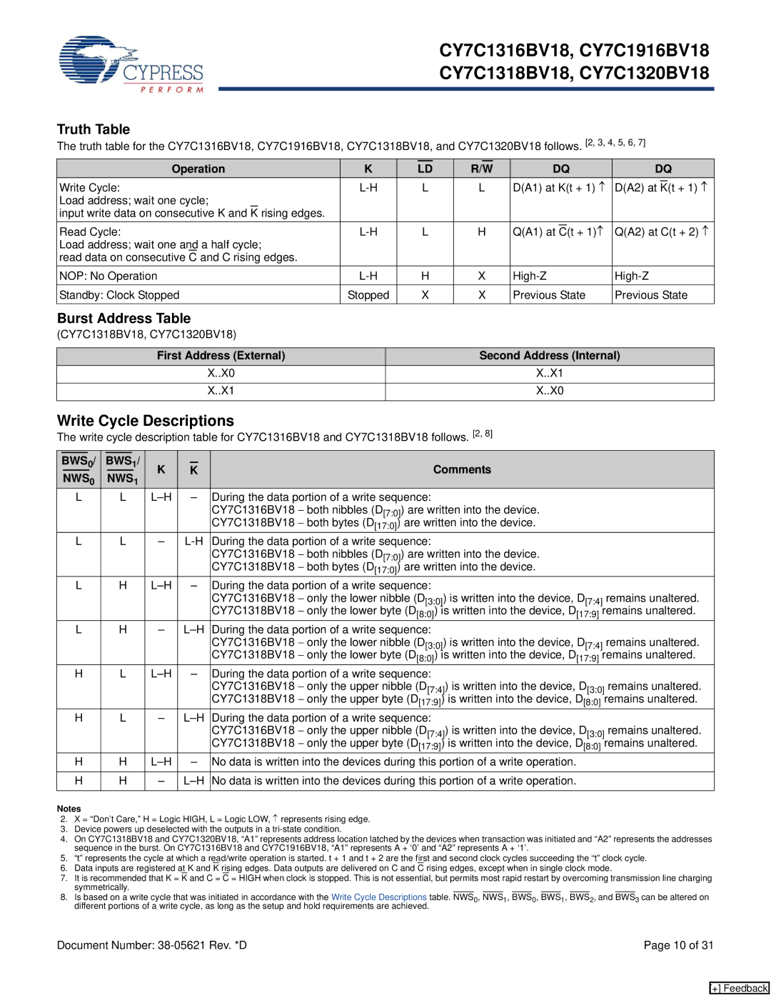
CY7C1316BV18, CY7C1916BV18, CY7C1320BV18, CY7C1318BV18 specifications
The Cypress CY7C1318BV18, CY7C1320BV18, CY7C1916BV18, and CY7C1316BV18 are advanced synchronous static RAM (SRAM) devices designed to meet the high-performance requirements of modern computing systems. Offering a blend of high speed, low power consumption, and large storage capacities, these chips are widely utilized in applications such as networking equipment, telecommunications, and high-speed data processing.The CY7C1318BV18 is a 2 Megabit SRAM that operates at a 2.5V supply voltage. It features a fast access time of 10ns, making it an excellent choice for systems that require rapid data retrieval. Its asynchronous interface simplifies integration into a wide range of devices. In terms of power efficiency, the CY7C1318BV18 has a low operating current, ensuring that it can be utilized in battery-powered applications without significantly draining power.
Similarly, the CY7C1320BV18 offers a larger 256 Kbit capacity while maintaining the same low-voltage operation and performance characteristics. This chip also features a synchronous interface, supporting high-speed data transfer rates that are ideal for networking and communication devices. The CY7C1320BV18's features include deep-write operation capabilities, enhancing its performance in write-intensive applications.
The CY7C1916BV18 takes performance a step further with its 32 Megabit capacity, suitable for applications requiring extensive memory resources. This device also supports advanced functions such as burst read modes, allowing for faster sequential data access. With its low-latency performance, the CY7C1916BV18 is an excellent choice for applications like digital signal processing and real-time data analysis.
Lastly, the CY7C1316BV18 is another variant offering 1 Megabit of storage. It combines high-speed functionality with low power usage, supporting a wide range of applications including consumer electronics and automotive systems. Its robust design ensures reliability under varying environmental conditions.
All of these SRAM devices incorporate Cypress’s advanced semiconductor technology, providing a combination of speed, efficiency, and reliability. They are available in various package options, which facilitate easy integration into diverse system designs. Overall, the Cypress CY7C1318BV18, CY7C1320BV18, CY7C1916BV18, and CY7C1316BV18 exemplify the company’s commitment to delivering high-quality memory solutions that cater to the evolving needs of the electronic industry.