CY7C1318CV18
CY7C1320CV18
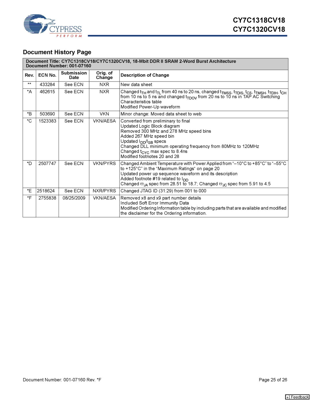
Document History Page
Document Title: CY7C1318CV18/CY7C1320CV18,
Document Number:
Rev. | ECN No. | Submission | Orig. of | Description of Change |
|
| Date | Change |
|
** | 433284 | See ECN | NXR | New data sheet |
|
|
|
|
|
*A | 462615 | See ECN | NXR | Changed tTH and tTL from 40 ns to 20 ns, changed tTMSS, tTDIS, tCS, tTMSH, tTDIH, tCH |
|
|
|
| from 10 ns to 5 ns and changed tTDOV from 20 ns to 10 ns in TAP AC Switching |
|
|
|
| Characteristics table |
|
|
|
| Modified |
*B | 503690 | See ECN | VKN | Minor change: Moved data sheet to web |
|
|
|
|
|
*C | 1523383 | See ECN | VKN/AESA | Converted from preliminary to final |
|
|
|
| Updated Logic Block diagram |
|
|
|
| Removed 300 MHz and 278 MHz speed bins |
|
|
|
| Added 267 MHz speed bin |
|
|
|
| Updated IDD/ISB specs |
|
|
|
| Changed DLL minimum operating frequency from 80MHz to 120MHz |
|
|
|
| Changed tCYC max spec to 8.4ns |
|
|
|
| Modified footnotes 20 and 28 |
*D | 2507747 | See ECN | VKN/PYRS | Changed Ambient Temperature with Power Applied from |
|
|
|
| to +125°C” in the “Maximum Ratings“ on page 20 |
|
|
|
| Updated power up sequence waveform and its description |
|
|
|
| Added footnote #19 related to IDD |
|
|
|
| Changed ΘJA spec from 28.51 to 18.7; Changed ΘJC spec from 5.91 to 4.5 |
*E | 2518624 | See ECN | NXR/PYRS | Changed JTAG ID (31:29) from 001 to 000 |
|
|
|
|
|
*F | 2755838 | 08/25/2009 | VKN/AESA | Removed x8 and x9 part number details |
|
|
|
| Included Soft Error Immunity Data |
|
|
|
| Modified Ordering Information table by including parts that are available and modified |
|
|
|
| the disclaimer for the Ordering information. |
Document Number: | Page 25 of 26 |
[+] Feedback