|
|
|
|
|
| CY7C1318CV18 | |
|
|
|
|
|
| CY7C1320CV18 | |
|
|
|
|
|
| ||
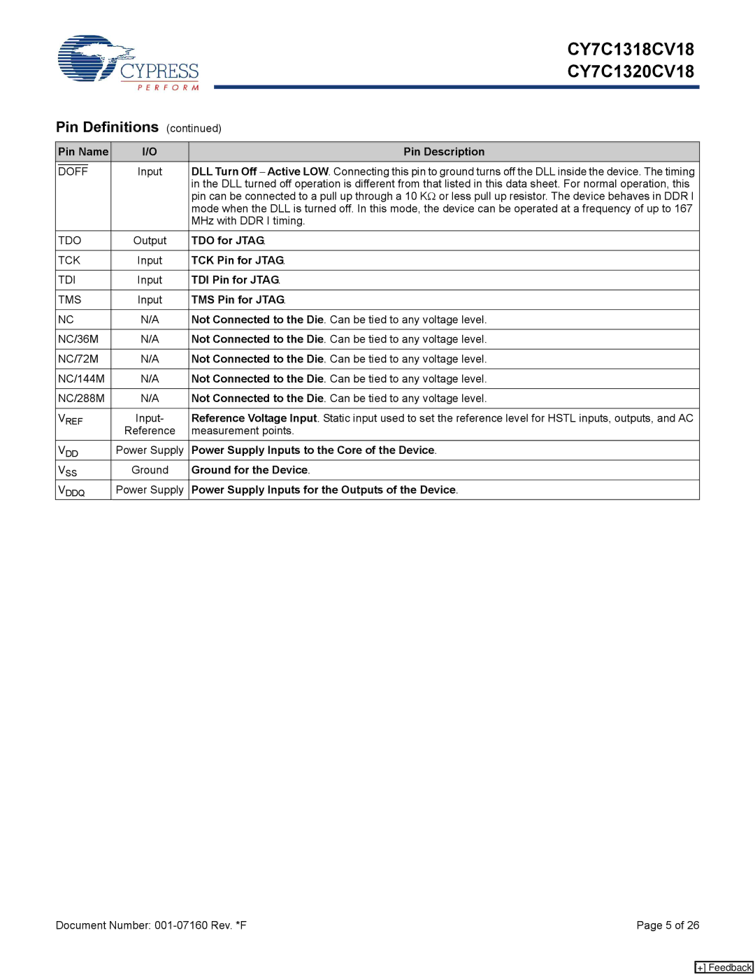
Pin Definitions (continued) | |||||||
|
|
|
|
|
| ||
| Pin Name | I/O |
|
| Pin Description | ||
|
|
| Input | DLL Turn Off − Active LOW. Connecting this pin to ground turns off the DLL inside the device. The timing | |||
| DOFF | ||||||
|
|
|
| in the DLL turned off operation is different from that listed in this data sheet. For normal operation, this | |||
|
|
|
| pin can be connected to a pull up through a 10 KΩ or less pull up resistor. The device behaves in DDR I | |||
|
|
|
| mode when the DLL is turned off. In this mode, the device can be operated at a frequency of up to 167 | |||
|
|
|
| MHz with DDR I timing. | |||
| TDO | Output | TDO for JTAG. | ||||
|
|
|
| ||||
| TCK | Input | TCK Pin for JTAG. | ||||
|
|
|
| ||||
| TDI | Input | TDI Pin for JTAG. | ||||
|
|
|
| ||||
| TMS | Input | TMS Pin for JTAG. | ||||
|
|
|
| ||||
| NC | N/A | Not Connected to the Die. Can be tied to any voltage level. | ||||
|
|
|
| ||||
| NC/36M | N/A | Not Connected to the Die. Can be tied to any voltage level. | ||||
|
|
|
| ||||
| NC/72M | N/A | Not Connected to the Die. Can be tied to any voltage level. | ||||
|
|
|
| ||||
| NC/144M | N/A | Not Connected to the Die. Can be tied to any voltage level. | ||||
|
|
|
| ||||
| NC/288M | N/A | Not Connected to the Die. Can be tied to any voltage level. | ||||
|
|
|
| ||||
| VREF | Input- | Reference Voltage Input. Static input used to set the reference level for HSTL inputs, outputs, and AC | ||||
|
|
| Reference | measurement points. | |||
| VDD | Power Supply | Power Supply Inputs to the Core of the Device. | ||||
| VSS | Ground | Ground for the Device. | ||||
| VDDQ | Power Supply | Power Supply Inputs for the Outputs of the Device. | ||||
Document Number: | Page 5 of 26 |
[+] Feedback
