|
|
|
| CY7C1330AV25 |
| ||
|
|
| PRELIMINARY | CY7C1332AV25 |
| ||
|
|
|
| ||||
|
|
|
|
|
|
|
|
|
|
|
|
|
|
|
|
TAP AC Switching Characteristics Over the Operating Range (continued)[10, 11] |
|
|
|
| |||
Parameter |
|
| Description | Min. | Max. | Unit |
|
|
|
|
|
|
| ||
tCH | Capture Hold after Clock Rise | 5 |
| ns |
| ||
Output Times |
|
|
|
|
|
|
|
|
|
|
|
|
| ||
tTDOV | TCK Clock LOW to TDO Valid |
| 10 | ns |
| ||
tTDOX | TCK Clock LOW to TDO Invalid | 0 |
| ns |
| ||
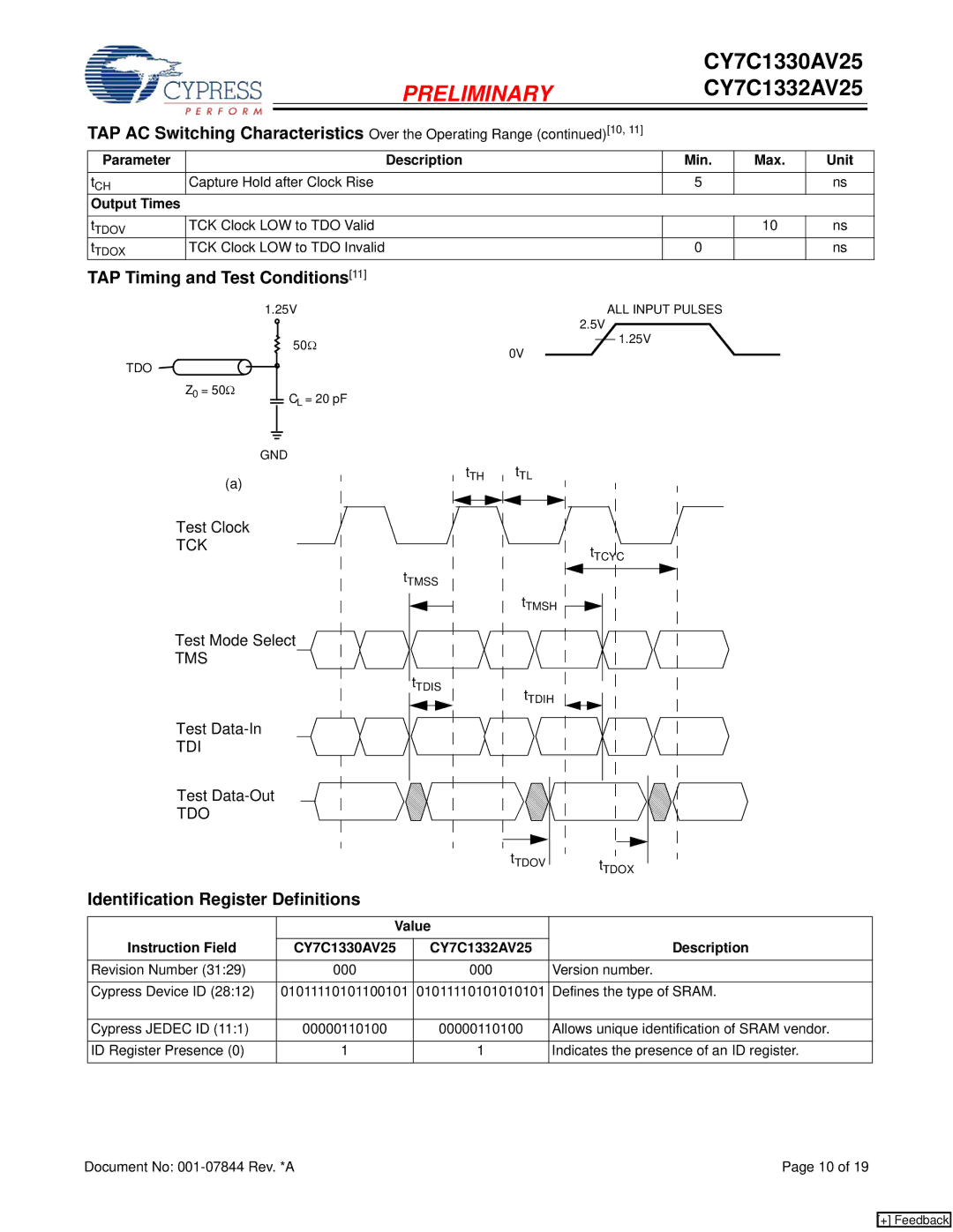
TAP Timing and Test Conditions[11]
|
|
| 1.25V | ||||||
|
|
|
|
|
|
|
|
| 50Ω |
|
|
|
|
|
|
|
|
| |
|
|
|
|
|
|
|
|
| |
TDO |
|
|
|
|
|
|
|
|
|
Z0 | = 50Ω |
|
|
|
|
|
| CL = 20 pF | |
|
|
|
|
|
| ||||
|
|
|
|
|
|
| |||
|
|
|
|
|
|
|
|
| |
|
|
|
|
|
|
|
|
|
|
|
|
|
|
|
|
|
|
|
|
|
|
|
|
|
|
|
|
|
|
GND
(a)
Test Clock
TCK
tTMSS
Test Mode Select
TMS
tTDIS
Test
TDI
Test
TDO
tTH
ALL INPUT PULSES
2.5V
1.25V
0V
tTL
tTCYC
tTMSH
tTDIH
tTDOV tTDOX
Identification Register Definitions
| Value |
| |
Instruction Field | CY7C1330AV25 | CY7C1332AV25 | Description |
|
|
|
|
Revision Number (31:29) | 000 | 000 | Version number. |
|
|
|
|
Cypress Device ID (28:12) | 01011110101100101 | 01011110101010101 | Defines the type of SRAM. |
|
|
|
|
Cypress JEDEC ID (11:1) | 00000110100 | 00000110100 | Allows unique identification of SRAM vendor. |
|
|
|
|
ID Register Presence (0) | 1 | 1 | Indicates the presence of an ID register. |
|
|
|
|
Document No: | Page 10 of 19 |
[+] Feedback