CY7C1330AV25
PRELIMINARYCY7C1332AV25
Features
•Fast clock speed: 250, 200 MHz
•Fast access time: 2.0, 2.25 ns
•Synchronous Pipelined Operation with
•Internally synchronized registered outputs eliminate the need to control OE
•2.5V core supply voltage
•
— Wide range HSTL I/O Levels
•Single Differential HSTL clock Input K and K
•Single WE (READ/WRITE) control pin
•Individual byte write (BWS[a:d]) control (may be tied LOW)
•Common I/O
•Asynchronous Output Enable Input
•Programmable Impedance Output Drivers
•JTAG boundary scan for BGA packaging version
•Available in a
Functional Description
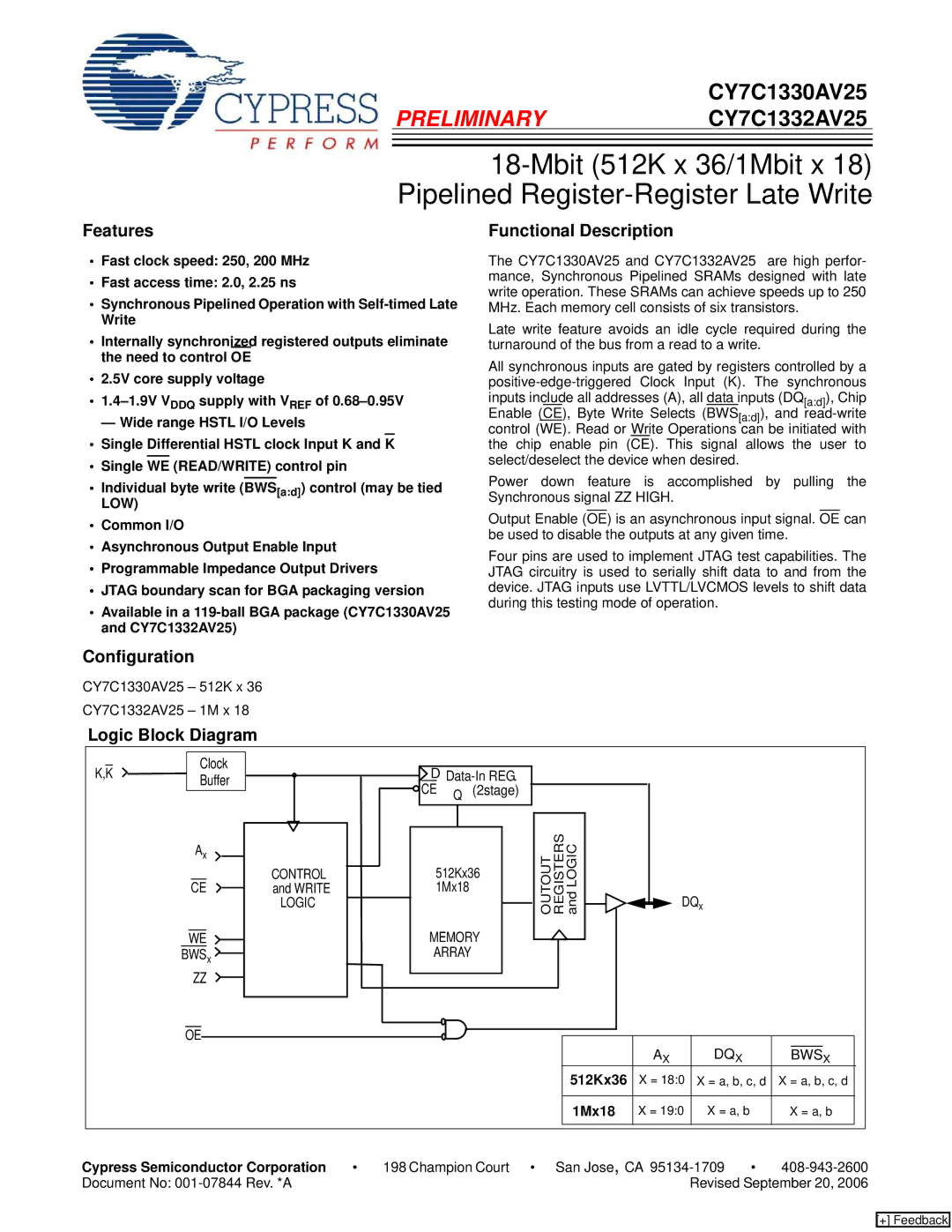
The CY7C1330AV25 and CY7C1332AV25 are high perfor- mance, Synchronous Pipelined SRAMs designed with late write operation. These SRAMs can achieve speeds up to 250 MHz. Each memory cell consists of six transistors.
Late write feature avoids an idle cycle required during the turnaround of the bus from a read to a write.
All synchronous inputs are gated by registers controlled by a
Power down feature is accomplished by pulling the Synchronous signal ZZ HIGH.
Output Enable (OE) is an asynchronous input signal. OE can be used to disable the outputs at any given time.
Four pins are used to implement JTAG test capabilities. The JTAG circuitry is used to serially shift data to and from the device. JTAG inputs use LVTTL/LVCMOS levels to shift data during this testing mode of operation.
Configuration
CY7C1330AV25 – 512K x 36
CY7C1332AV25 – 1M x 18
Logic Block Diagram
Clock
K,K ![]()
![]()
![]() Buffer
Buffer
Ax |
| CONTROL | |
| |||
|
|
| |
CE |
|
| and WRITE |
|
| ||
|
|
| LOGIC |
WE
BWSx ![]()
![]()
ZZ
![]()
![]() D
D
![]()
![]() CE Q (2stage)
CE Q (2stage)
512Kx36
1Mx18
MEMORY
ARRAY
OUTOUT REGISTERS and LOGIC
DQx
OE
| AX | DQX |
|
| X |
|
| BWS | |||
512Kx36 | X = 18:0 | X = a, b, c, d | X = a, b, c, d | ||
|
|
|
|
|
|
1Mx18 | X = 19:0 | X = a, b | X = a, b | ||
|
|
|
|
|
|
Cypress Semiconductor Corporation | • | 198 Champion Court • San Jose, CA | • | |
Document No: |
| Revised September 20, 2006 | ||
[+] Feedback