|
|
|
|
|
|
|
|
|
|
|
|
|
|
| CY7C1330AV25 |
| ||
|
|
|
|
|
|
|
|
|
| PRELIMINARY |
|
| CY7C1332AV25 |
| ||||
|
|
|
|
|
|
|
|
|
|
| ||||||||
|
|
|
|
|
|
|
|
|
|
|
|
|
|
|
|
|
|
|
|
|
|
|
|
|
|
|
|
|
|
|
|
|
|
|
|
| |
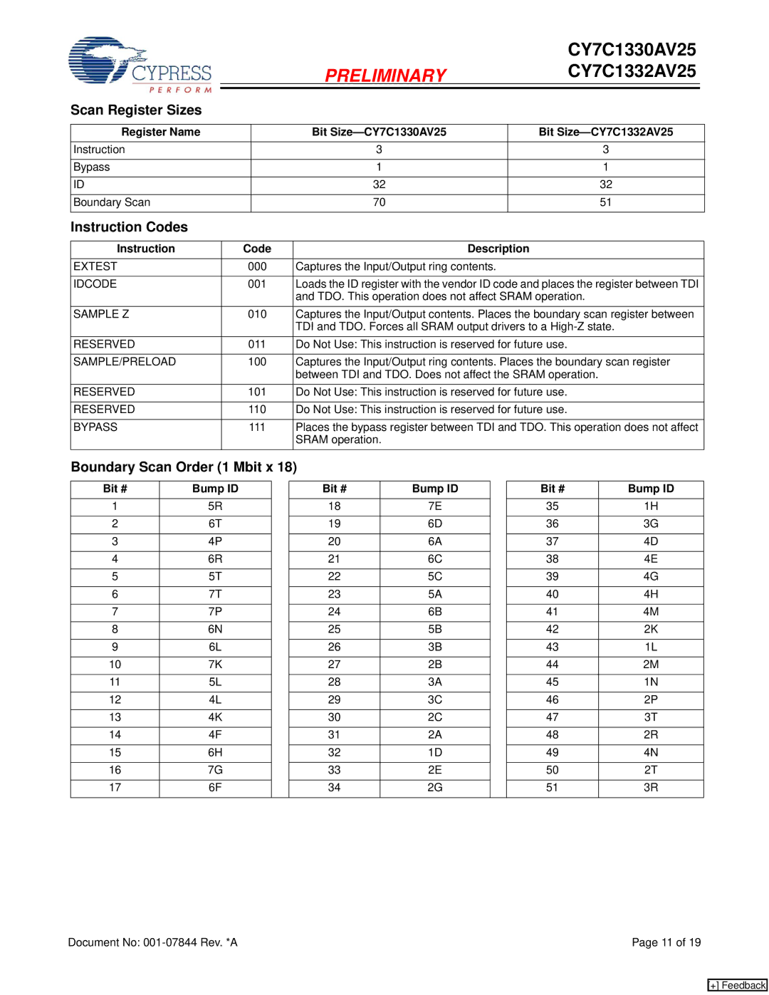
Scan Register Sizes |
|
|
|
|
|
|
|
|
|
|
|
|
| |||||
|
|
|
|
|
|
|
|
|
|
|
|
|
| |||||
Register Name |
|
|
|
| Bit |
|
| Bit |
| |||||||||
Instruction |
|
|
|
|
|
|
|
| 3 |
|
|
| 3 |
|
| |||
|
|
|
|
|
|
|
|
|
|
|
|
|
|
|
|
|
|
|
Bypass |
|
|
|
|
|
|
|
| 1 |
|
|
| 1 |
|
| |||
|
|
|
|
|
|
|
|
|
|
|
|
|
|
|
|
|
|
|
ID |
|
|
|
|
|
|
|
| 32 |
|
|
| 32 |
|
| |||
|
|
|
|
|
|
|
|
|
|
|
|
|
|
|
|
|
|
|
Boundary Scan |
|
|
|
|
|
|
|
| 70 |
|
|
| 51 |
|
| |||
|
|
|
|
|
|
|
|
|
|
|
|
|
|
|
|
|
|
|
Instruction Codes |
|
|
|
|
|
|
|
|
|
|
|
|
|
|
|
|
| |
|
|
|
|
|
|
|
|
|
|
|
|
|
|
|
|
|
| |
Instruction |
|
|
|
| Code |
|
|
| Description |
|
| |||||||
EXTEST |
|
|
|
| 000 |
|
| Captures the Input/Output ring contents. |
|
| ||||||||
|
|
|
|
|
|
|
|
|
|
|
|
|
|
| ||||
IDCODE |
|
|
|
| 001 |
|
| Loads the ID register with the vendor ID code and places the register between TDI |
| |||||||||
|
|
|
|
|
|
|
|
|
| and TDO. This operation does not affect SRAM operation. |
|
| ||||||
SAMPLE Z |
|
|
|
| 010 |
|
| Captures the Input/Output contents. Places the boundary scan register between |
| |||||||||
|
|
|
|
|
|
|
|
|
| TDI and TDO. Forces all SRAM output drivers to a |
|
| ||||||
RESERVED |
|
|
|
| 011 |
|
| Do Not Use: This instruction is reserved for future use. |
|
| ||||||||
|
|
|
|
|
|
|
|
|
|
|
|
|
|
| ||||
SAMPLE/PRELOAD |
|
|
|
| 100 |
|
| Captures the Input/Output ring contents. Places the boundary scan register |
| |||||||||
|
|
|
|
|
|
|
|
|
| between TDI and TDO. Does not affect the SRAM operation. |
|
| ||||||
RESERVED |
|
|
|
| 101 |
|
| Do Not Use: This instruction is reserved for future use. |
|
| ||||||||
|
|
|
|
|
|
|
|
|
|
|
|
|
|
|
| |||
RESERVED |
|
|
|
| 110 |
|
| Do Not Use: This instruction is reserved for future use. |
|
| ||||||||
|
|
|
|
|
|
|
|
|
|
|
|
|
|
| ||||
BYPASS |
|
|
|
| 111 |
|
| Places the bypass register between TDI and TDO. This operation does not affect |
| |||||||||
|
|
|
|
|
|
|
|
|
| SRAM operation. |
|
|
|
|
|
|
| |
Boundary Scan Order (1 Mbit x 18) |
|
|
|
|
|
|
| |||||||||||
|
|
|
|
|
|
|
|
|
|
|
|
|
|
|
| |||
Bit # |
| Bump ID |
|
|
|
| Bit # |
| Bump ID |
|
| Bit # |
| Bump ID |
| |||
|
|
|
|
|
|
|
|
|
|
|
|
|
|
|
| |||
1 |
| 5R |
|
|
|
| 18 |
| 7E |
|
| 35 |
| 1H |
| |||
|
|
|
|
|
|
|
|
|
|
|
|
|
|
|
| |||
2 |
| 6T |
|
|
|
| 19 |
| 6D |
|
| 36 |
| 3G |
| |||
|
|
|
|
|
|
|
|
|
|
|
|
|
|
|
| |||
3 |
| 4P |
|
|
|
| 20 |
| 6A |
|
| 37 |
| 4D |
| |||
|
|
|
|
|
|
|
|
|
|
|
|
|
|
|
| |||
4 |
| 6R |
|
|
|
| 21 |
| 6C |
|
| 38 |
| 4E |
| |||
|
|
|
|
|
|
|
|
|
|
|
|
|
|
|
| |||
5 |
| 5T |
|
|
|
| 22 |
| 5C |
|
| 39 |
| 4G |
| |||
|
|
|
|
|
|
|
|
|
|
|
|
|
|
|
| |||
6 |
| 7T |
|
|
|
| 23 |
| 5A |
|
| 40 |
| 4H |
| |||
|
|
|
|
|
|
|
|
|
|
|
|
|
|
|
| |||
7 |
| 7P |
|
|
|
| 24 |
| 6B |
|
| 41 |
| 4M |
| |||
|
|
|
|
|
|
|
|
|
|
|
|
|
|
|
| |||
8 |
| 6N |
|
|
|
| 25 |
| 5B |
|
| 42 |
| 2K |
| |||
|
|
|
|
|
|
|
|
|
|
|
|
|
|
|
| |||
9 |
| 6L |
|
|
|
| 26 |
| 3B |
|
| 43 |
| 1L |
| |||
|
|
|
|
|
|
|
|
|
|
|
|
|
|
|
| |||
10 |
| 7K |
|
|
|
| 27 |
| 2B |
|
| 44 |
| 2M |
| |||
|
|
|
|
|
|
|
|
|
|
|
|
|
|
|
| |||
11 |
| 5L |
|
|
|
| 28 |
| 3A |
|
| 45 |
| 1N |
| |||
|
|
|
|
|
|
|
|
|
|
|
|
|
|
|
| |||
12 |
| 4L |
|
|
|
| 29 |
| 3C |
|
| 46 |
| 2P |
| |||
|
|
|
|
|
|
|
|
|
|
|
|
|
|
|
| |||
13 |
| 4K |
|
|
|
| 30 |
| 2C |
|
| 47 |
| 3T |
| |||
|
|
|
|
|
|
|
|
|
|
|
|
|
|
|
| |||
14 |
| 4F |
|
|
|
| 31 |
| 2A |
|
| 48 |
| 2R |
| |||
|
|
|
|
|
|
|
|
|
|
|
|
|
|
|
| |||
15 |
| 6H |
|
|
|
| 32 |
| 1D |
|
| 49 |
| 4N |
| |||
|
|
|
|
|
|
|
|
|
|
|
|
|
|
|
| |||
16 |
| 7G |
|
|
|
| 33 |
| 2E |
|
| 50 |
| 2T |
| |||
|
|
|
|
|
|
|
|
|
|
|
|
|
|
|
| |||
17 |
| 6F |
|
|
|
| 34 |
| 2G |
|
| 51 |
| 3R |
| |||
|
|
|
|
|
|
|
|
|
|
|
|
|
|
|
|
|
|
|
Document No: | Page 11 of 19 |
[+] Feedback