CY7C1330AV25
PRELIMINARYCY7C1332AV25
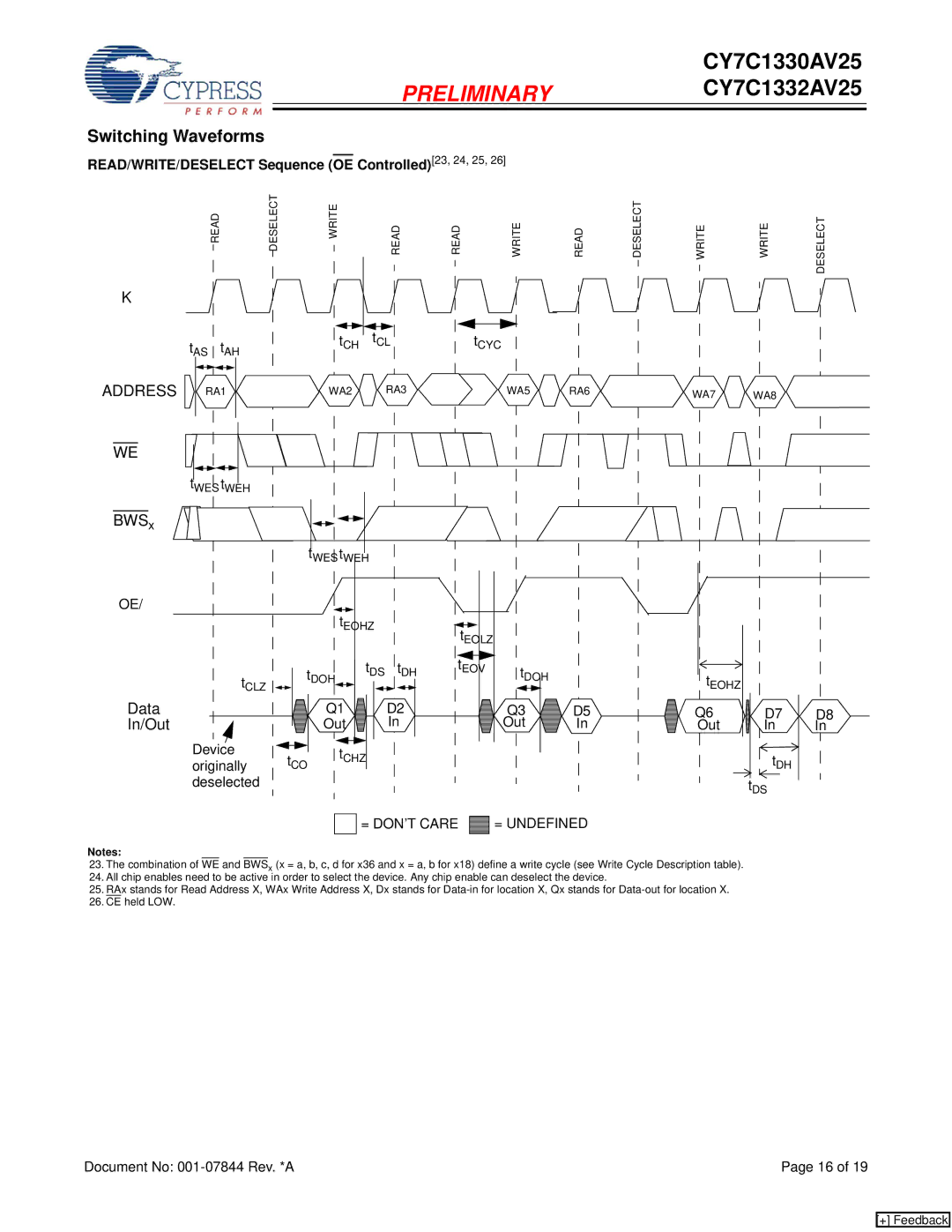
Switching Waveforms
READ/WRITE/DESELECT Sequence (OE Controlled)[23, 24, 25, 26]
READ | DESELECT | WRITE | |||
|
|
|
| ||
|
|
|
|
|
|
K
|
|
|
|
|
|
|
|
|
|
|
|
| tAS |
| tAH |
|
|
| tCH | ||||
|
|
|
|
| |||||||
|
| ||||||||||
|
|
|
|
| |||||||
ADDRESS |
|
|
|
|
|
|
|
|
|
|
|
|
|
|
|
|
|
|
|
|
|
| |
|
|
|
|
|
|
|
|
|
|
| |
| RA1 |
|
|
|
|
|
|
| |||
| WA2 | ||||||||||
|
|
|
|
|
|
|
|
|
|
|
|
|
|
|
|
|
|
|
|
|
|
|
|
READ | READ | WRITE | READ | DESELECT | WRITE | WRITE | DESELECT | ||||
|
|
|
|
|
|
|
|
|
|
| |
|
|
|
|
|
|
|
|
|
|
| |
|
|
|
|
|
|
|
|
|
|
| |
|
|
|
|
|
|
|
|
|
|
|
|
|
|
|
|
|
|
|
|
|
|
|
|
|
|
|
|
|
|
|
|
|
|
|
|
|
|
|
|
|
|
|
|
|
|
|
|
|
|
|
|
|
|
|
|
|
|
|
|
|
|
|
|
|
|
|
|
tCL |
|
| t |
|
|
|
|
|
|
|
|
| ||||
|
|
|
|
|
| CYC |
|
|
|
|
|
|
|
|
| |
|
|
|
|
|
|
|
|
|
|
|
|
|
|
|
|
|
|
|
|
|
|
|
|
|
|
|
|
|
|
|
|
|
|
|
| RA3 |
|
|
| WA5 |
| RA6 |
| WA7 | WA8 | |||||
|
|
| ||||||||||||||
|
|
|
|
|
|
|
|
|
| |||||||
|
|
|
|
|
|
|
|
|
|
|
|
|
|
|
|
|
|
|
|
|
|
|
|
|
|
|
|
|
|
|
|
|
|
|
|
|
|
|
|
|
|
|
|
|
|
|
|
|
|
|
WE
tWES tWEH
BWSx
tWES tWEH
OE/ | tEOHZ |
|
|
|
|
|
|
|
| |
|
|
| tEOLZ |
|
|
|
|
| ||
|
|
|
|
|
|
|
|
|
| |
| t | DS | t | DH | tEOV | tDOH |
|
|
|
|
tCLZ | tDOH |
|
|
| tEOHZ |
|
| |||
|
|
|
|
|
|
|
|
| ||
Data | Q1 |
| D2 |
| Q3 | D5 | Q6 | D7 | D8 | |
In/Out | Out |
| In |
|
| Out | In | Out | In | In |
Device | tCHZ |
|
|
|
|
|
|
| tDH |
|
originally | tCO |
|
|
|
|
|
|
|
| |
deselected |
|
|
|
|
|
|
|
| tDS |
|
= DON’T CARE  = UNDEFINED
Notes:
23.The combination of WE and BWSx (x = a, b, c, d for x36 and x = a, b for x18) define a write cycle (see Write Cycle Description table).
24.All chip enables need to be active in order to select the device. Any chip enable can deselect the device.
25.RAx stands for Read Address X, WAx Write Address X, Dx stands for
26.CE held LOW.
Document No: | Page 16 of 19 |
[+] Feedback