CY7C1364C
Burst Sequences
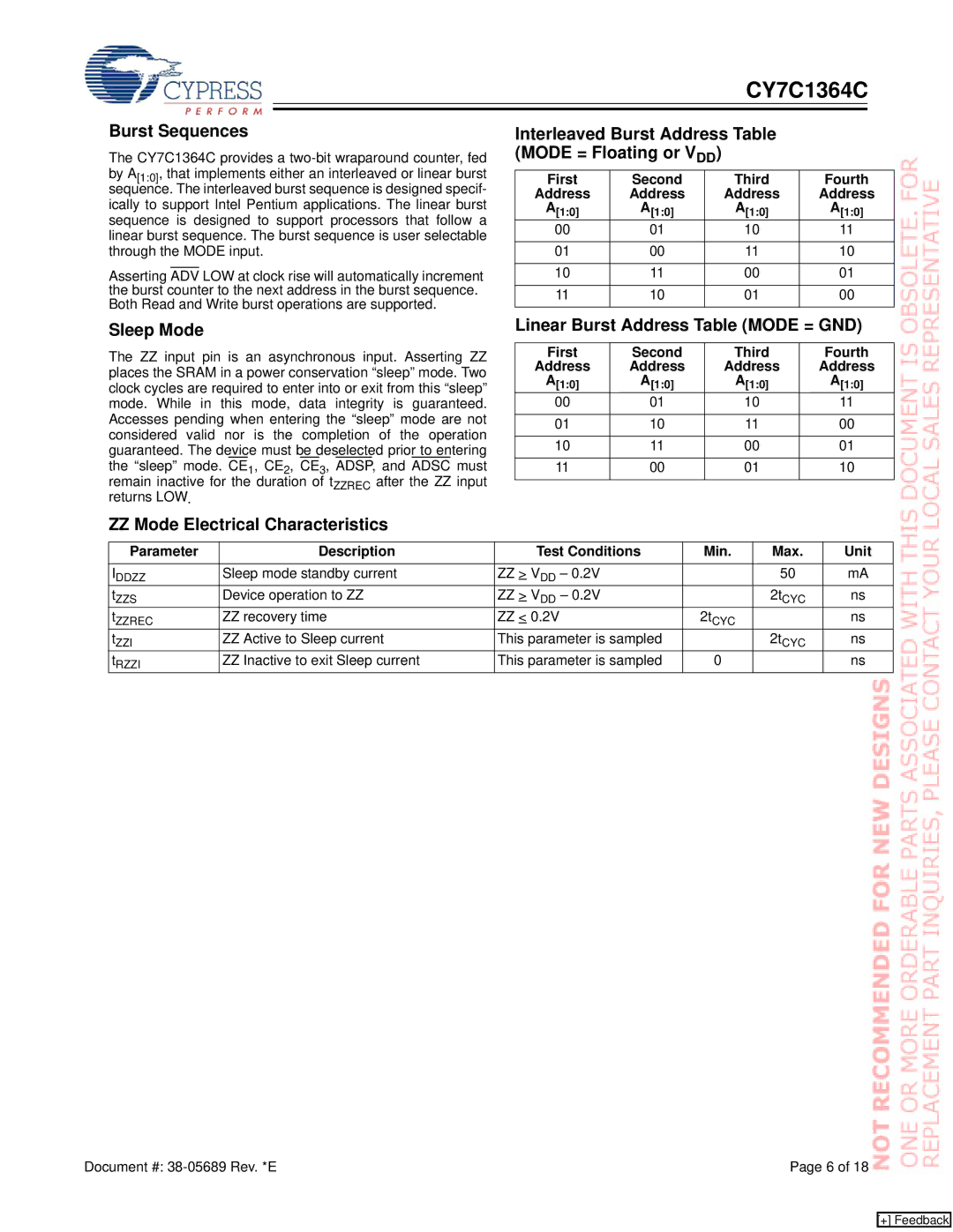
The CY7C1364C provides a
Asserting ADV LOW at clock rise will automatically increment the burst counter to the next address in the burst sequence. Both Read and Write burst operations are supported.
Sleep Mode
The ZZ input pin is an asynchronous input. Asserting ZZ places the SRAM in a power conservation “sleep” mode. Two clock cycles are required to enter into or exit from this “sleep” mode. While in this mode, data integrity is guaranteed. Accesses pending when entering the “sleep” mode are not considered valid nor is the completion of the operation guaranteed. The device must be deselected prior to entering the “sleep” mode. CE1, CE2, CE3, ADSP, and ADSC must remain inactive for the duration of tZZREC after the ZZ input returns LOW.
ZZ Mode Electrical Characteristics
Interleaved Burst Address Table (MODE = Floating or VDD)
First | Second | Third | Fourth |
Address | Address | Address | Address |
A[1:0] | A[1:0] | A[1:0] | A[1:0] |
00 | 01 | 10 | 11 |
|
|
|
|
01 | 00 | 11 | 10 |
|
|
|
|
10 | 11 | 00 | 01 |
|
|
|
|
11 | 10 | 01 | 00 |
|
|
|
|
Linear Burst Address Table (MODE = GND)
First | Second | Third | Fourth |
Address | Address | Address | Address |
A[1:0] | A[1:0] | A[1:0] | A[1:0] |
00 | 01 | 10 | 11 |
|
|
|
|
01 | 10 | 11 | 00 |
|
|
|
|
10 | 11 | 00 | 01 |
|
|
|
|
11 | 00 | 01 | 10 |
|
|
|
|
Parameter | Description | Test Conditions | Min. | Max. | Unit |
IDDZZ | Sleep mode standby current | ZZ > VDD – 0.2V |
| 50 | mA |
tZZS | Device operation to ZZ | ZZ > VDD – 0.2V |
| 2tCYC | ns |
tZZREC | ZZ recovery time | ZZ < 0.2V | 2tCYC |
| ns |
tZZI | ZZ Active to Sleep current | This parameter is sampled |
| 2tCYC | ns |
tRZZI | ZZ Inactive to exit Sleep current | This parameter is sampled | 0 |
| ns |
Document #: | Page 6 of 18 |
[+] Feedback