|
|
|
|
|
|
|
|
|
|
|
|
|
|
|
|
|
|
|
| CY7C1364C | |||||
|
|
|
|
|
|
|
|
|
|
|
|
|
|
|
|
| |||||||||
|
|
|
|
|
|
|
|
|
|
|
|
|
|
|
|
|
|
|
|
|
|
|
|
|
|
|
|
|
|
|
|
|
|
|
|
|
|
|
|
|
|
|
|
|
|
|
|
|
|
|
|
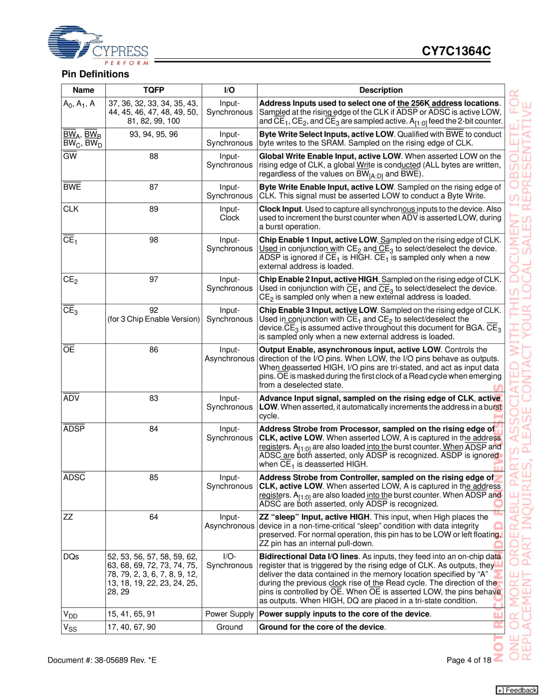
| Pin Definitions |
|
|
|
|
|
|
|
|
|
| ||||||||||||||
|
|
|
|
|
|
|
|
| |||||||||||||||||
|
| Name | TQFP | I/O |
|
| Description | ||||||||||||||||||
|
|
|
|
|
|
| |||||||||||||||||||
|
| A0, A1, A | 37, 36, 32, 33, 34, 35, 43, | Input- | Address Inputs used to select one of the 256K address locations. | ||||||||||||||||||||
|
|
|
|
|
|
|
|
|
|
|
|
| 44, 45, 46, 47, 48, 49, 50, | Synchronous | Sampled at the rising edge of the CLK if ADSP or ADSC is active LOW, | ||||||||||
|
|
|
|
|
|
|
|
|
|
|
|
| 81, 82, 99, 100 |
| and CE1, CE2, and CE3 are sampled active. A[1:0] feed the | ||||||||||
|
|
|
|
| A, |
|
|
| B | 93, 94, 95, 96 | Input- | Byte Write Select Inputs, active LOW. Qualified with |
| to conduct | |||||||||||
|
| BW | BW | BWE | |||||||||||||||||||||
|
| BWC, BWD |
|
|
| Synchronous | byte writes to the SRAM. Sampled on the rising edge of CLK. | ||||||||||||||||||
|
|
|
|
|
|
|
|
|
|
| 88 | Input- | Global Write Enable Input, active LOW. When asserted LOW on the | ||||||||||||
|
| GW | |||||||||||||||||||||||
|
|
|
|
|
|
|
|
|
|
|
|
|
|
|
| Synchronous | rising edge of CLK, a global Write is conducted (ALL bytes are written, | ||||||||
|
|
|
|
|
|
|
|
|
|
|
|
|
|
|
|
| regardless of the values on BW[A:D] and BWE). | ||||||||
|
|
|
|
|
|
|
|
|
|
| 87 | Input- | Byte Write Enable Input, active LOW. Sampled on the rising edge of | ||||||||||||
|
| BWE | |||||||||||||||||||||||
|
|
|
|
|
|
|
|
|
|
|
|
|
|
|
| Synchronous | CLK. This signal must be asserted LOW to conduct a Byte Write. | ||||||||
|
| CLK | 89 | Input- | Clock Input. Used to capture all synchronous inputs to the device. Also | ||||||||||||||||||||
|
|
|
|
|
|
|
|
|
|
|
|
|
|
|
| Clock | used to increment the burst counter when ADV is asserted LOW, during | ||||||||
|
|
|
|
|
|
|
|
|
|
|
|
|
|
|
|
| a burst operation. | ||||||||
|
|
| 1 |
|
|
| 98 | Input- | Chip Enable 1 Input, active LOW. Sampled on the rising edge of CLK. | ||||||||||||||||
|
| CE | |||||||||||||||||||||||
|
|
|
|
|
|
|
|
|
|
|
|
|
|
|
| Synchronous | Used in conjunction with CE2 and | CE3 to select/deselect the device. | |||||||
|
|
|
|
|
|
|
|
|
|
|
|
|
|
|
|
| ADSP is ignored if CE1 is HIGH. CE1 is sampled only when a new | ||||||||
|
|
|
|
|
|
|
|
|
|
|
|
|
|
|
|
| external address is loaded. | ||||||||
|
| CE2 | 97 | Input- | Chip Enable 2 Input, active HIGH. Sampled on the rising edge of CLK. | ||||||||||||||||||||
|
|
|
|
|
|
|
|
|
|
|
|
|
|
|
| Synchronous | Used in conjunction with CE1 and CE3 to select/deselect the device. | ||||||||
|
|
|
|
|
|
|
|
|
|
|
|
|
|
|
|
| CE2 is sampled only when a new external address is loaded. | ||||||||
|
|
| 3 |
|
|
| 92 | Input- | Chip Enable 3 Input, active LOW. Sampled on the rising edge of CLK. | ||||||||||||||||
|
| CE | |||||||||||||||||||||||
|
|
|
|
|
|
|
|
|
|
|
|
| (for 3 Chip Enable Version) | Synchronous | Used in conjunction with CE1 and CE2 to select/deselect the |
|
| ||||||||
|
|
|
|
|
|
|
|
|
|
|
|
|
|
|
|
| device.CE3 is assumed active throughout this document for BGA. CE3 | ||||||||
|
|
|
|
|
|
|
|
|
|
|
|
|
|
|
|
| is sampled only when a new external address is loaded. | ||||||||
|
|
|
|
|
|
|
| 86 | Input- | Output Enable, asynchronous input, active LOW. Controls the | |||||||||||||||
|
| OE | |||||||||||||||||||||||
|
|
|
|
|
|
|
|
|
|
|
|
|
|
|
| Asynchronous | direction of the I/O pins. When LOW, the I/O pins behave as outputs. | ||||||||
|
|
|
|
|
|
|
|
|
|
|
|
|
|
|
|
| When deasserted HIGH, I/O pins are | ||||||||
|
|
|
|
|
|
|
|
|
|
|
|
|
|
|
|
| pins. OE is masked during the first clock of a Read cycle when emerging | ||||||||
|
|
|
|
|
|
|
|
|
|
|
|
|
|
|
|
| from a deselected state. | ||||||||
|
|
|
|
|
|
|
|
|
| 83 | Input- | Advance Input signal, sampled on the rising edge of CLK, active | |||||||||||||
|
| ADV | |||||||||||||||||||||||
|
|
|
|
|
|
|
|
|
|
|
|
|
|
|
| Synchronous | LOW. When asserted, it automatically increments the address in a burst | ||||||||
|
|
|
|
|
|
|
|
|
|
|
|
|
|
|
|
| cycle. | ||||||||
|
|
|
|
|
|
|
|
|
|
|
| 84 | Input- | Address Strobe from Processor, sampled on the rising edge of | |||||||||||
|
| ADSP | |||||||||||||||||||||||
|
|
|
|
|
|
|
|
|
|
|
|
|
|
|
| Synchronous | CLK, active LOW. When asserted LOW, A is captured in the address | ||||||||
|
|
|
|
|
|
|
|
|
|
|
|
|
|
|
|
| registers. A[1:0] are also loaded into the burst counter. When ADSP and | ||||||||
|
|
|
|
|
|
|
|
|
|
|
|
|
|
|
|
| ADSC are both asserted, only ADSP is recognized. ASDP is ignored | ||||||||
|
|
|
|
|
|
|
|
|
|
|
|
|
|
|
|
| when | CE | 1 is deasserted HIGH. | ||||||
|
|
|
|
|
|
|
|
|
|
|
| 85 | Input- | Address Strobe from Controller, sampled on the rising edge of | |||||||||||
|
| ADSC | |||||||||||||||||||||||
|
|
|
|
|
|
|
|
|
|
|
|
|
|
|
| Synchronous | CLK, active LOW. When asserted LOW, A is captured in the address | ||||||||
|
|
|
|
|
|
|
|
|
|
|
|
|
|
|
|
| registers. A[1:0] are also loaded into the burst counter. When ADSP and | ||||||||
|
|
|
|
|
|
|
|
|
|
|
|
|
|
|
|
| ADSC are both asserted, only ADSP is recognized. | ||||||||
|
| ZZ | 64 | Input- | ZZ “sleep” Input, active HIGH. This input, when High places the | ||||||||||||||||||||
|
|
|
|
|
|
|
|
|
|
|
|
|
|
|
| Asynchronous | device in a | ||||||||
|
|
|
|
|
|
|
|
|
|
|
|
|
|
|
|
| preserved. For normal operation, this pin has to be LOW or left floating. | ||||||||
|
|
|
|
|
|
|
|
|
|
|
|
|
|
|
|
| ZZ pin has an internal | ||||||||
|
| DQs | 52, 53, 56, 57, 58, 59, 62, | I/O- | Bidirectional Data I/O lines. As inputs, they feed into an | ||||||||||||||||||||
|
|
|
|
|
|
|
|
|
|
|
|
| 63, 68, 69, 72, 73, 74, 75, | Synchronous | register that is triggered by the rising edge of CLK. As outputs, they | ||||||||||
|
|
|
|
|
|
|
|
|
|
|
|
| 78, 79, 2, 3, 6, 7, 8, 9, 12, |
| deliver the data contained in the memory location specified by “A” | ||||||||||
|
|
|
|
|
|
|
|
|
|
|
|
| 13, 18, 19, 22, 23, 24, 25, |
| during the previous clock rise of the Read cycle. The direction of the | ||||||||||
|
|
|
|
|
|
|
|
|
|
|
|
| 28, 29 |
|
|
| pins is controlled by OE. When OE is asserted LOW, the pins behave | ||||||||
|
|
|
|
|
|
|
|
|
|
|
|
|
|
|
|
| as outputs. When HIGH, DQ are placed in a | ||||||||
|
| VDD | 15, 41, 65, 91 | Power Supply | Power supply inputs to the core of the device. | ||||||||||||||||||||
|
| VSS | 17, 40, 67, 90 | Ground | Ground for the core of the device. | ||||||||||||||||||||
Document #: |
|
|
|
|
| Page 4 of 18 | |||||||||||||||||||
[+] Feedback