CY7C1365C
Timing Diagrams (continued)
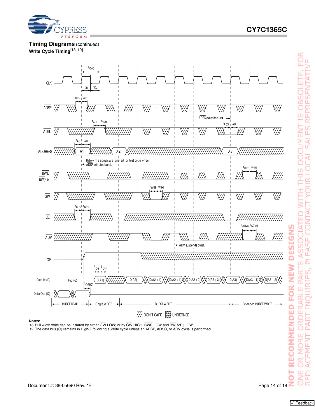
Write Cycle Timing[18, 19]
tCYC
CLK
tCH tCL
tADS tADH
ADSP
tADS tADH
ADSC
tAS tAH
ADDRESS ![]() A1
A1 ![]()
![]() A2
A2
Byte write signals are ignored for first cycle when
![]() ADSP initiates burst.
ADSP initiates burst.
BWE,
BW[A:D]
t t
WES WEH
ADSC extends burst.
tADS tADH
A3
tWES tWEH
GW
tCES tCEH
CE
ADV
OE
Data in (D) |
Data Out (Q)
tOEHZ
tDS t DH
D(A1)
tADVS tADVH
![]() ADV suspends burst.
ADV suspends burst.
D(A2) | D(A2 + 1) | D(A2 + 1) | D(A2 + 2) | D(A2 + 3) | D(A3) | D(A3 + 1) | D(A3 + 2) |
BURST READ
Single WRITE | BURST WRITE | Extended BURST WRITE |
DON’T CARE | UNDEFINED |
Notes:
18.Full width write can be initiated by either GW LOW; or by GW HIGH, BWE LOW and BW[A:D] LOW.
19.The data bus (Q) remains in
Document #: | Page 14 of 18 |
[+] Feedback