CY7C1365C
Timing Diagrams (continued)
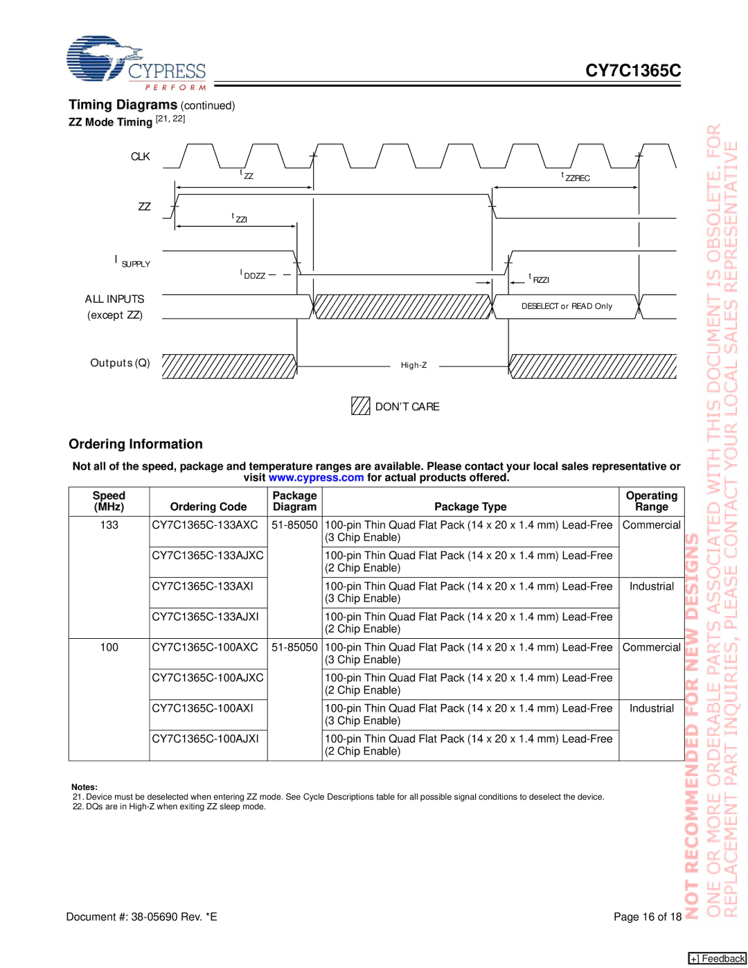
ZZMode Timing [21, 22]
CLK
t ZZ
ZZ
t ZZI
ISUPPLY
I DDZZ
ALL INPUTS (except ZZ)
Outputs (Q)
Ordering Information

 DON’T CARE
t ZZREC
t RZZI
DESELECT or READ Only
Not all of the speed, package and temperature ranges are available. Please contact your local sales representative or
visit www.cypress.com for actual products offered.
Speed | Ordering Code | Package | Package Type | Operating |
(MHz) | Diagram | Range | ||
|
|
|
|
|
133 | Commercial | |||
|
|
| (3 Chip Enable) |
|
|
|
| ||
|
|
| (2 Chip Enable) |
|
|
| Industrial | ||
|
|
| (3 Chip Enable) |
|
|
|
| ||
|
|
| (2 Chip Enable) |
|
100 | Commercial | |||
|
|
| (3 Chip Enable) |
|
|
|
| ||
|
|
| (2 Chip Enable) |
|
|
| Industrial | ||
|
|
| (3 Chip Enable) |
|
|
|
| ||
|
|
| (2 Chip Enable) |
|
Notes:
21.Device must be deselected when entering ZZ mode. See Cycle Descriptions table for all possible signal conditions to deselect the device.
22.DQs are in
Document #: | Page 16 of 18 |
[+] Feedback