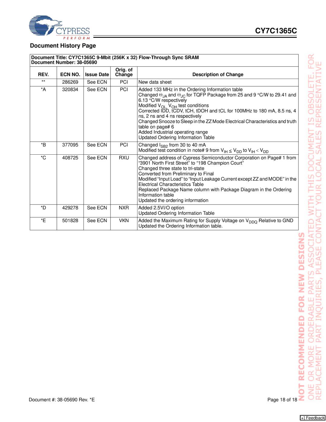
CY7C1365C
Document History Page
Document Title: CY7C1365C
Document Number:
REV. | ECN NO. | Issue Date | Orig. of | Description of Change |
Change | ||||
|
|
|
|
|
** | 286269 | See ECN | PCI | New data sheet |
|
|
|
|
|
*A | 320834 | See ECN | PCI | Added 133 MHz in the Ordering Information table |
|
|
|
| Changed ΘJA and ΘJC for TQFP Package from 25 and 9 °C/W to 29.41 and |
|
|
|
| 6.13 °C/W respectively |
|
|
|
| Modified VOL, VOH test conditions |
|
|
|
| Corrected IDD, tCDV, tCH, tDOH and tCL for 100MHz to 180 mA, 8.5 ns, 4 |
|
|
|
| ns, 2 ns and 4 ns respectively |
|
|
|
| Changed Snooze to Sleep in the ZZ Mode Electrical Characteristics and truth |
|
|
|
| table on page# 6 |
|
|
|
| Added Industrial operating range |
|
|
|
| Updated Ordering Information Table |
*B | 377095 | See ECN | PCI | Changed ISB2 from 30 to 40 mA |
|
|
|
| Modified test condition in note# 9 from VIH < VDD to VIH < VDD |
*C | 408725 | See ECN | RXU | Changed address of Cypress Semiconductor Corporation on Page# 1 from |
|
|
|
| “3901 North First Street” to “198 Champion Court” |
|
|
|
| Changed three state to |
|
|
|
| Converted from Preliminary to Final |
|
|
|
| Modified “Input Load” to “Input Leakage Current except ZZ and MODE” in the |
|
|
|
| Electrical Characteristics Table |
|
|
|
| Replaced Package Name column with Package Diagram in the Ordering |
|
|
|
| Information table |
|
|
|
| Updated the ordering information |
*D | 429278 | See ECN | NXR | Added 2.5VI/O option |
|
|
|
| Updated Ordering Information Table |
*E | 501828 | See ECN | VKN | Added the Maximum Rating for Supply Voltage on VDDQ Relative to GND |
|
|
|
| Updated the Ordering Information table. |
Document #: | Page 18 of 18 |
[+] Feedback