CY7C1470V33
CY7C1472V33
CY7C1474V33
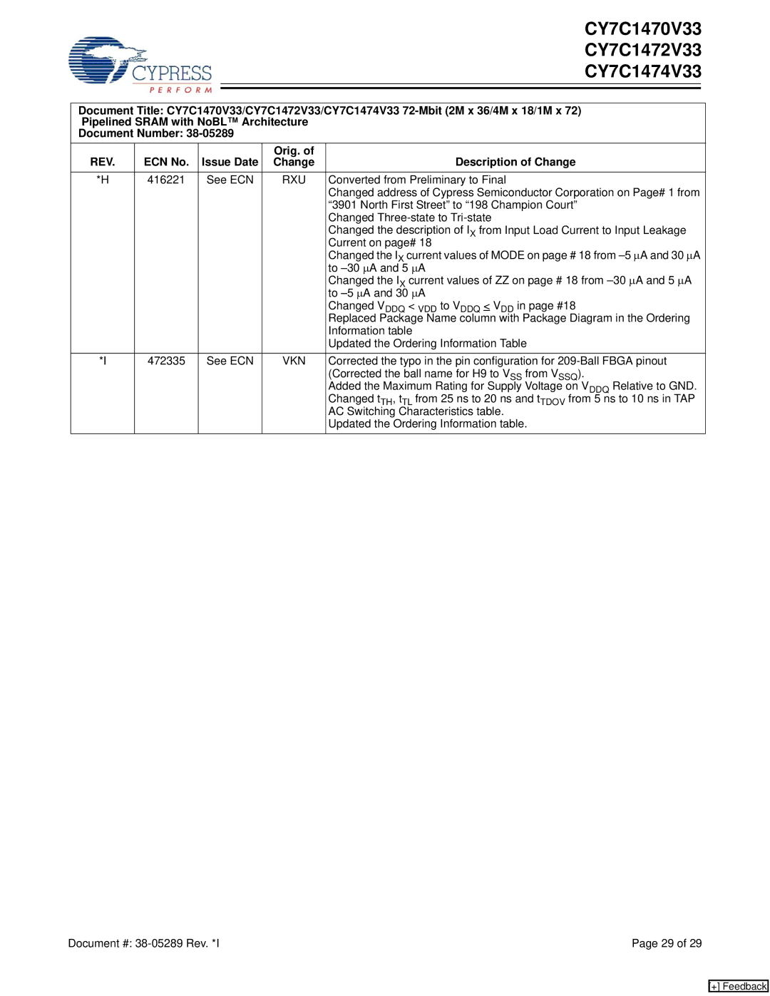
Document Title: CY7C1470V33/CY7C1472V33/CY7C1474V33
Document Number:
REV. | ECN No. | Issue Date | Orig. of | Description of Change |
Change | ||||
|
|
|
|
|
*H | 416221 | See ECN | RXU | Converted from Preliminary to Final |
|
|
|
| Changed address of Cypress Semiconductor Corporation on Page# 1 from |
|
|
|
| “3901 North First Street” to “198 Champion Court” |
|
|
|
| Changed |
|
|
|
| Changed the description of IX from Input Load Current to Input Leakage |
|
|
|
| Current on page# 18 |
|
|
|
| Changed the IX current values of MODE on page # 18 from |
|
|
|
| to |
|
|
|
| Changed the IX current values of ZZ on page # 18 from |
|
|
|
| to |
|
|
|
| Changed VDDQ < VDD to VDDQ < VDD in page #18 |
|
|
|
| Replaced Package Name column with Package Diagram in the Ordering |
|
|
|
| Information table |
|
|
|
| Updated the Ordering Information Table |
*I | 472335 | See ECN | VKN | Corrected the typo in the pin configuration for |
|
|
|
| (Corrected the ball name for H9 to VSS from VSSQ). |
|
|
|
| Added the Maximum Rating for Supply Voltage on VDDQ Relative to GND. |
|
|
|
| Changed tTH, tTL from 25 ns to 20 ns and tTDOV from 5 ns to 10 ns in TAP |
|
|
|
| AC Switching Characteristics table. |
|
|
|
| Updated the Ordering Information table. |
Document #: | Page 29 of 29 |
[+] Feedback
