CY7C1470V33
CY7C1472V33
CY7C1474V33
possible to capture all other signals and simply ignore the value of the CLK captured in the boundary scan register.
Once the data is captured, it is possible to shift out the data by putting the TAP into the
Note that since the PRELOAD part of the command is not implemented, putting the TAP to the
BYPASS
When the BYPASS instruction is loaded in the instruction register and the TAP is placed in a
Reserved
These instructions are not implemented but are reserved for future use. Do not use these instructions.
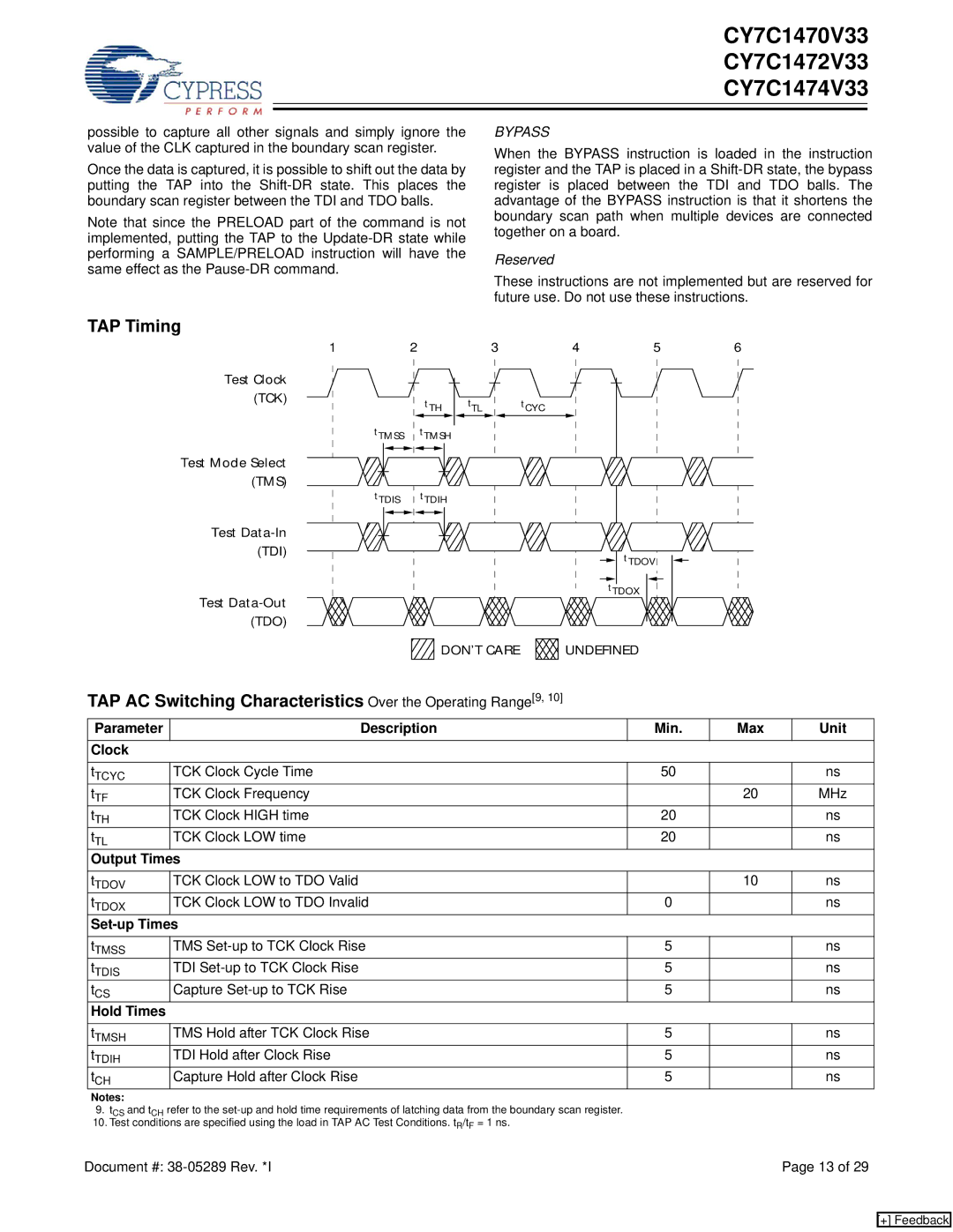
TAP Timing
12
Test Clock
(TCK)tTH
tTMSS tTMSH
Test Mode Select (TMS)
tTDIS tTDIH
Test
3 | 4 | 5 | 6 |
tTL tCYC
tTDOV
tTDOX
Test |
|
(TDO) |
|
DON’T CARE | UNDEFINED |
TAP AC Switching Characteristics Over the Operating Range[9, 10]
Parameter | Description | Min. | Max | Unit |
Clock |
|
|
|
|
|
|
|
|
|
tTCYC | TCK Clock Cycle Time | 50 |
| ns |
tTF | TCK Clock Frequency |
| 20 | MHz |
tTH | TCK Clock HIGH time | 20 |
| ns |
tTL | TCK Clock LOW time | 20 |
| ns |
Output Times |
|
|
| |
tTDOV | TCK Clock LOW to TDO Valid |
| 10 | ns |
tTDOX | TCK Clock LOW to TDO Invalid | 0 |
| ns |
|
|
|
| |
tTMSS | TMS | 5 |
| ns |
tTDIS | TDI | 5 |
| ns |
tCS | Capture | 5 |
| ns |
Hold Times |
|
|
|
|
|
|
|
|
|
tTMSH | TMS Hold after TCK Clock Rise | 5 |
| ns |
tTDIH | TDI Hold after Clock Rise | 5 |
| ns |
tCH | Capture Hold after Clock Rise | 5 |
| ns |
Notes:
9.tCS and tCH refer to the
10. Test conditions are specified using the load in TAP AC Test Conditions. tR/tF = 1 ns.
Document #: | Page 13 of 29 |
[+] Feedback