CY7C1471BV33 CY7C1473BV33, CY7C1475BV33
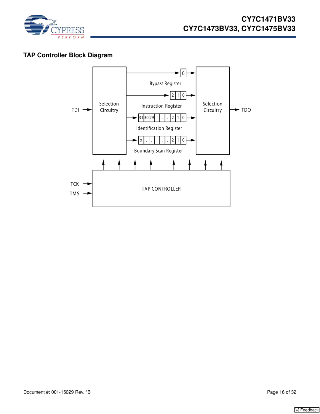
TAP Controller Block Diagram
TDI |
|
| Selection |
|
| Circuitry | |
| |||
|
|
|
|
|
|
|
|
|
|
|
|
|
|
|
|
|
|
|
|
|
|
|
|
|
|
|
|
|
|
|
| 0 |
|
|
|
|
|
|
|
|
|
|
|
|
|
|
|
|
|
| |
|
|
|
| Bypass Register |
|
|
|
| |||||||
|
|
|
|
|
|
|
|
|
|
|
|
|
|
|
|
|
|
|
|
|
|
|
|
| 2 | 1 |
| 0 |
|
| Selection |
|
|
|
|
|
|
|
|
|
|
|
| ||||
|
|
|
|
|
|
|
|
|
|
|
|
|
|
| |
|
| Instruction Register |
|
|
| ||||||||||
|
|
|
|
| Circuitry | ||||||||||
|
|
|
|
|
|
|
|
|
|
|
|
|
|
| |
|
| 31 | 30 | 29 | . | . | . | 2 | 1 |
| 0 |
|
|
| |
|
|
|
|
|
| ||||||||||
|
|
|
|
|
|
|
|
|
|
|
|
|
|
| |
| Identification Register |
| |||||||||||||
|
|
|
|
|
|
|
|
|
| ||||||
|
| x | . | . | . | . | . | 2 | 1 |
| 0 |
|
|
| |
|
|
|
|
|
| ||||||||||
|
|
|
|
|
|
|
|
|
|
|
|
|
|
| |
| Boundary Scan Register |
| |||||||||||||
TDO
TCK
TM S
TAP CONTROLLER
Document #: | Page 16 of 32 |
[+] Feedback