CY7C1546V18, CY7C1557V18
CY7C1548V18, CY7C1550V18
TAP AC Switching Characteristics
Over the Operating Range [12, 14]
Parameter | Description | Min | Max | Unit |
tTCYC | TCK Clock Cycle Time | 50 |
| ns |
tTF | TCK Clock Frequency |
| 20 | MHz |
tTH | TCK Clock HIGH | 20 |
| ns |
tTL | TCK Clock LOW | 20 |
| ns |
Setup Times |
|
|
|
|
|
|
|
|
|
tTMSS | TMS Setup to TCK Clock Rise | 5 |
| ns |
tTDIS | TDI Setup to TCK Clock Rise | 5 |
| ns |
tCS | Capture Setup to TCK Rise | 5 |
| ns |
Hold Times |
|
|
|
|
tTMSH | TMS Hold after TCK Clock Rise | 5 |
| ns |
tTDIH | TDI Hold after Clock Rise | 5 |
| ns |
tCH | Capture Hold after Clock Rise | 5 |
| ns |
Output Times |
|
|
|
|
|
|
|
|
|
tTDOV | TCK Clock LOW to TDO Valid |
| 10 | ns |
tTDOX | TCK Clock LOW to TDO Invalid | 0 |
| ns |
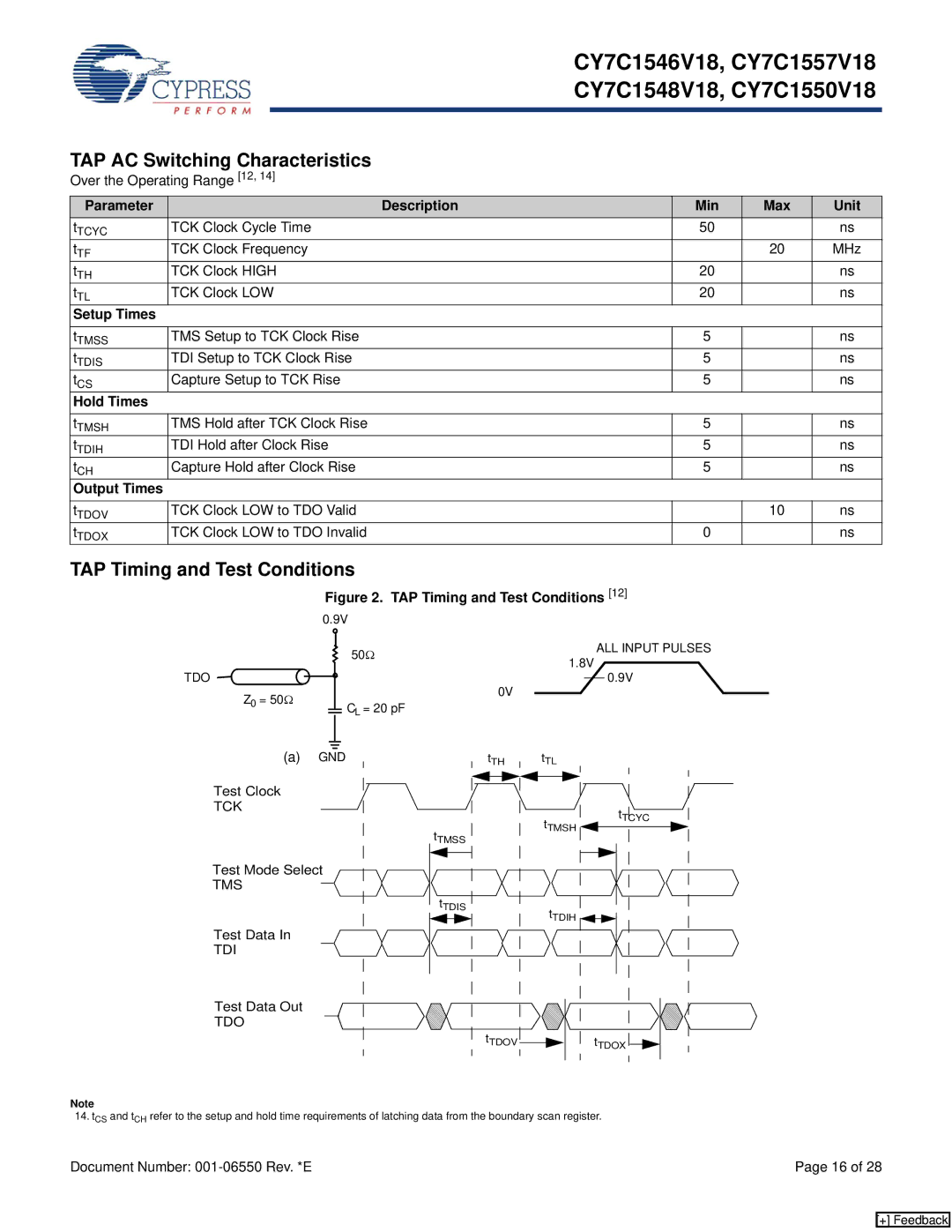
TAP Timing and Test Conditions
Figure 2. TAP Timing and Test Conditions [12]
|
|
| 0.9V |
|
|
|
| |||||||||
|
|
|
|
|
|
|
|
|
| 50Ω |
|
|
|
| ||
|
|
|
|
|
|
|
|
|
|
|
|
|
| |||
|
|
|
|
|
|
|
|
|
|
|
|
|
| |||
TDO |
|
|
|
|
|
|
|
|
|
|
|
|
|
| 0V | |
Z0 | = 50Ω |
|
|
|
|
|
|
|
|
|
|
|
| |||
|
|
|
|
|
|
|
|
|
|
|
| |||||
|
|
|
|
|
|
|
|
|
|
|
|
| ||||
|
|
|
|
|
|
|
| CL = 20 pF |
|
|
|
| ||||
|
|
|
|
|
|
|
|
|
|
|
|
|
| |||
|
|
|
|
|
|
|
|
|
|
|
|
|
| |||
|
|
|
|
|
|
|
|
|
|
|
|
|
| |||
|
|
|
|
|
|
|
|
|
|
|
|
|
|
| ||
|
|
|
|
|
|
|
|
|
|
|
| |||||
|
|
|
|
|
|
|
|
|
| |||||||
|
| (a) GND |
|
|
| tTH | ||||||||||
|
|
|
| |||||||||||||
|
|
|
|
|
|
|
|
|
|
|
|
|
|
|
|
|
Test Clock
TCK
tTMSS
ALL INPUT PULSES
1.8V
0.9V
tTL
tTMSH ![]() tTCYC
tTCYC
Test Mode Select
TMS
Test Data In
TDI
Test Data Out
TDO
Note
tTDIS | tTDIH |
|
tTDOV |
|
|
|
| t |
|
|
|
| ||
|
|
|
| ||
|
|
|
| ||
| |||||
|
|
|
|
| TDOX |
14. tCS and tCH refer to the setup and hold time requirements of latching data from the boundary scan register.
Document Number: | Page 16 of 28 |
[+] Feedback