CY7C1566V18, CY7C1577V18
CY7C1568V18, CY7C1570V18
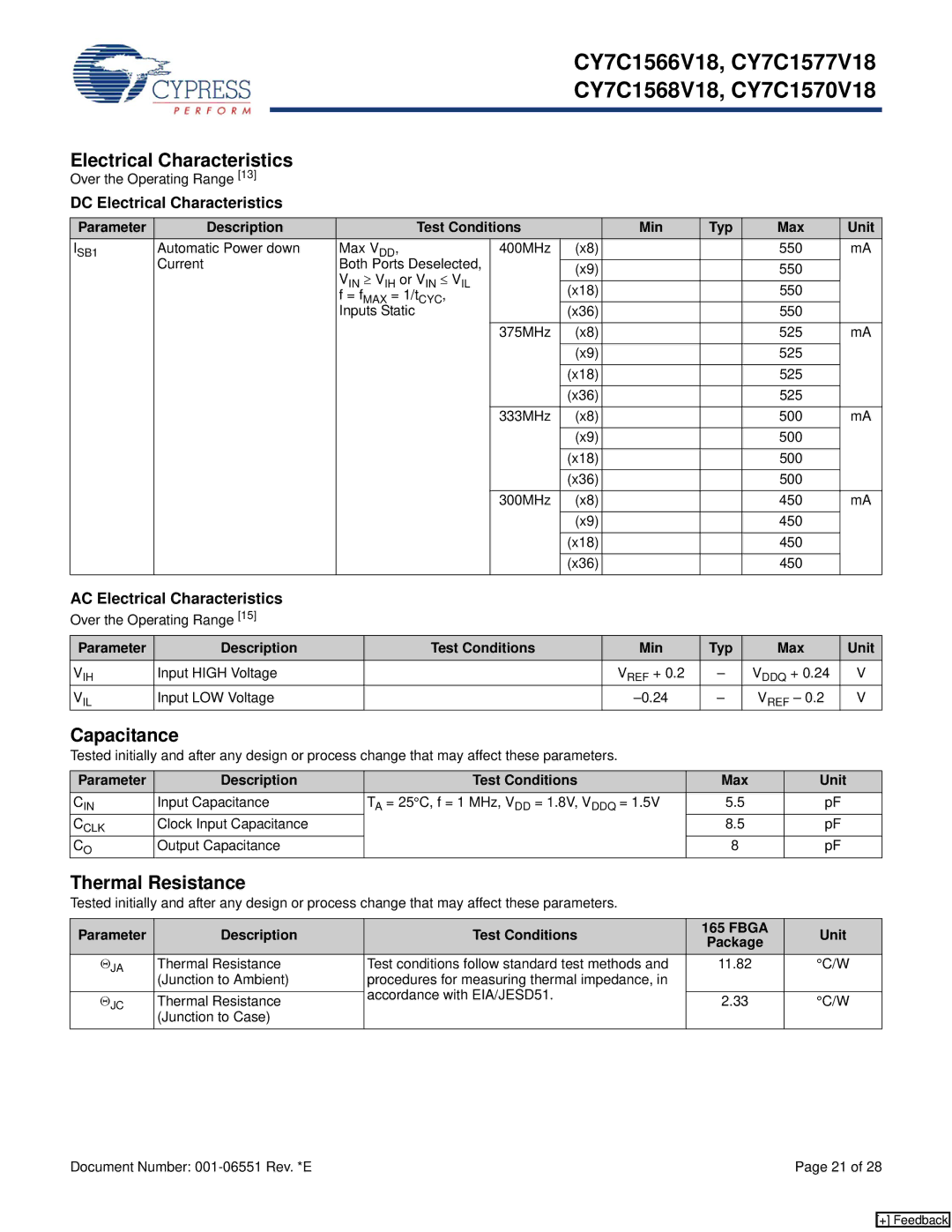
Electrical Characteristics
Over the Operating Range [13]
DC Electrical Characteristics
Parameter | Description | Test Conditions |
| Min | Typ | Max | Unit | |
ISB1 | Automatic Power down | Max VDD, | 400MHz | (x8) |
|
| 550 | mA |
| Current | Both Ports Deselected, |
|
|
|
|
|
|
|
| (x9) |
|
| 550 |
| ||
|
| VIN ≥ VIH or VIN ≤ VIL |
|
|
|
| ||
|
|
| (x18) |
|
| 550 |
| |
|
| f = fMAX = 1/tCYC, |
|
|
|
| ||
|
| Inputs Static |
| (x36) |
|
| 550 |
|
|
|
| 375MHz | (x8) |
|
| 525 | mA |
|
|
|
| (x9) |
|
| 525 |
|
|
|
|
| (x18) |
|
| 525 |
|
|
|
|
| (x36) |
|
| 525 |
|
|
|
| 333MHz | (x8) |
|
| 500 | mA |
|
|
|
| (x9) |
|
| 500 |
|
|
|
|
| (x18) |
|
| 500 |
|
|
|
|
| (x36) |
|
| 500 |
|
|
|
| 300MHz | (x8) |
|
| 450 | mA |
|
|
|
| (x9) |
|
| 450 |
|
|
|
|
| (x18) |
|
| 450 |
|
|
|
|
| (x36) |
|
| 450 |
|
AC Electrical Characteristics
Over the Operating Range [15]
Parameter | Description | Test Conditions | Min | Typ | Max | Unit |
VIH | Input HIGH Voltage |
| VREF + 0.2 | – | VDDQ + 0.24 | V |
VIL | Input LOW Voltage |
| – | VREF – 0.2 | V |
Capacitance
Tested initially and after any design or process change that may affect these parameters.
Parameter | Description | Test Conditions | Max | Unit |
CIN | Input Capacitance | TA = 25°C, f = 1 MHz, VDD = 1.8V, VDDQ = 1.5V | 5.5 | pF |
CCLK | Clock Input Capacitance |
| 8.5 | pF |
CO | Output Capacitance |
| 8 | pF |
Thermal Resistance
Tested initially and after any design or process change that may affect these parameters.
Parameter | Description | Test Conditions | 165 FBGA | Unit | |
Package | |||||
|
|
|
| ||
ΘJA | Thermal Resistance | Test conditions follow standard test methods and | 11.82 | °C/W | |
| (Junction to Ambient) | procedures for measuring thermal impedance, in |
|
| |
|
| accordance with EIA/JESD51. |
|
| |
ΘJC | Thermal Resistance | 2.33 | °C/W | ||
| |||||
| (Junction to Case) |
|
|
|
Document Number: | Page 21 of 28 |
[+] Feedback