Contents
EZ-USB AT2LP USB 2.0 to ATA/ATAPI Bridge
Features
Block Diagram
CY7C68300C/CY7C68301C CY7C68320C/CY7C68321C
CY4615C EZ-USB AT2LP Reference Design Kit USB Specification version
Applications
CY7C68300A Compatibility
Introduction
56-pin SSOP
EZ-USB AT2LP
CY7C68300C
CY7C68301C
DD13
EZ-USB AT2LP CY7C68300C CY7C68301C 56-pin QFN
ENABLE
RESET#
56-pin SSOP
EZ-USB AT2LP
CY7C68320C
CY7C68321C
DD15
EZ-USB AT2LP CY7C68320C CY7C68321C 56-pin QFN
ARESET#
GPIO2
CY7C68321A
100-pin TQFP
CY7C68320A
PU 10K
USB D+ signal See “DPLUS, DMINUS” on page
USB D-signal See “DPLUS, DMINUS” on page
page
CY7C68320C/CY7C68321C
CY7C68300C/CY7C68301C
VBUS detection See “VBUSATAENABLE” on
Chip reset See “RESET#” on page
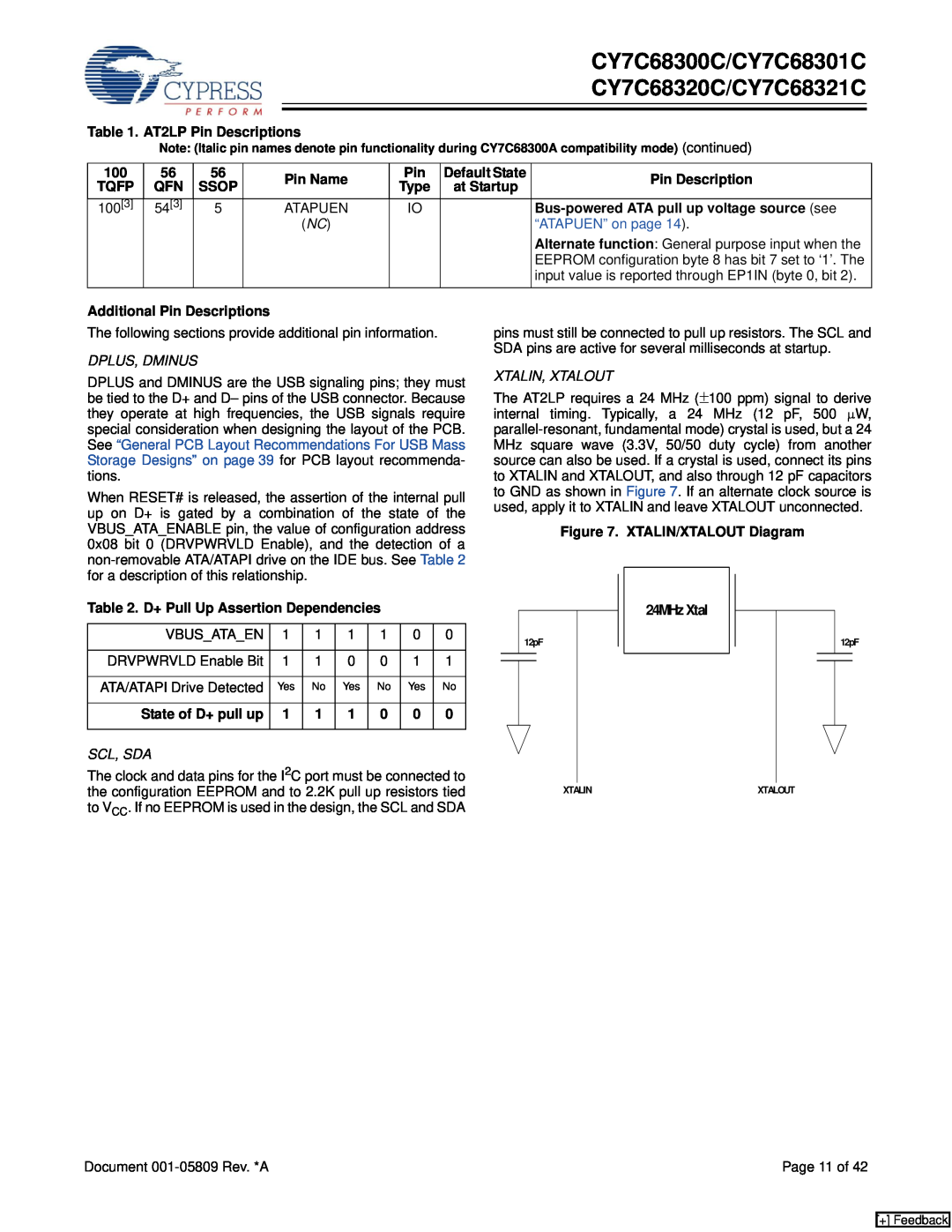
XTALIN, XTALOUT
“ATAPUEN” on page
DPLUS, DMINUS
SCL, SDA
USB High-Speed
SYSIRQ
LOWPWR#
GPIO Pins
ATA Interface Pins
DRVPWRVLD
PWR500#
VBUSATAENABLE
RESET#
ATAPUEN
ATA Command Block ATACB
HID Functions for Button Controls
Functional Overview
Field Description
Table 6. ATACB Field Descriptions
Byte
Field Name
5-12
Figure 10. Operational Mode Selection Flow
Operating Modes
Operational Mode Selection Flow
Normal Mass Storage Mode
Bulk-Only Transport Specification . There is a vendor-specific
Table 7. Command Block Wrapper
Fused Memory Data
MfgCB
Figure 11. Snapshot of ‘AT2LP Blaster’ Utility
EEPROM Organization
length. This allows the CY7C68300C/CY7C68301C to work
Enable a delay of up to 120 ms at each read of the DRQ bit
where the device data length does not match the host data
“Functional Overview” on page 15 for more detail on how
Determines if the AT2LP is to do an SRST reset during drive
returned on bits 2, 1, and 0 of EP1IN. This bit must be set to
CY7C68300C/CY7C68301C CY7C68320C/CY7C68321C
does not exist. The USB Mass Storage Class Bulk-Only
Configuration
USB Bulk In Endpoint
Interface Descriptor
USB Bulk Out Endpoint
Terminator
Page 29 of
Number of the channel, must be a zero based value that is
Descriptor-Index 0 LANGID
CY7C68300C/CY7C68301C CY7C68320C/CY7C68321C
unique serial
Descriptor-Serial Number
LOADCONFIGDATA
bmRequestType
Table 12.EEPROM-related Vendor-specific Commands
READCONFIGDATA
Label
Operating Conditions
DC Characteristics
Absolute Maximum Ratings
USB Transceiver Characteristics
AC Electrical Characteristics
Ordering Information
ATA Timing Characteristics
Figure 12. 100-Pin Thin Plastic Quad Flatpack 14 x 20 x 1.4 mm A101
Package Diagrams
Figure 13. 56-lead Shrunk Small Outline Package
Package Diagrams continued
Page 39 of
General PCB Layout Recommendations For USB Mass Storage Designs
Figure 14. 56-Lead QFN 8 x 8 mm LF56A
PCB Material
Quad Flat Package No Leads QFN Package Design Notes
Other Design Considerations
Devices With Small Buffers
Disclaimers, Trademarks, and Copyrights
IDE Removable Media Devices
ECN NO
Document History Paged
Issue Date
Document Number