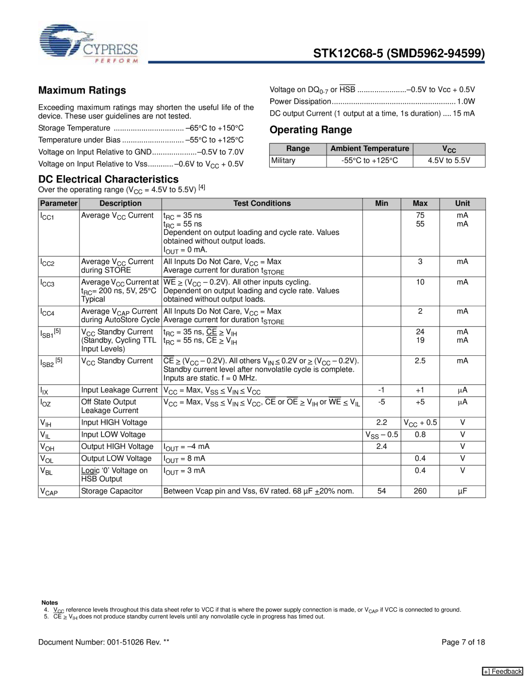
Maximum Ratings
Exceeding maximum ratings may shorten the useful life of the device. These user guidelines are not tested.
Storage Temperature | |
Temperature under Bias | |
Voltage on Input Relative to GND | |
Voltage on Input Relative to Vss |
|
|
|
Voltage on | ||
Power Dissipation | 1.0W | |
DC output Current (1 output at a time, 1s duration) .... 15 mA
Operating Range
Range | Ambient Temperature | VCC |
Military | 4.5V to 5.5V | |
|
|
|
DC Electrical Characteristics
Over the operating range (VCC = 4.5V to 5.5V) [4]
Parameter | Description |
|
|
|
|
| Test Conditions | Min | Max | Unit | |||||||
ICC1 | Average VCC Current | tRC = 35 ns |
| 75 | mA | ||||||||||||
|
|
|
| tRC = 55 ns |
| 55 | mA | ||||||||||
|
|
|
| Dependent on output loading and cycle rate. Values |
|
|
| ||||||||||
|
|
|
| obtained without output loads. |
|
|
| ||||||||||
|
|
|
| IOUT = 0 mA. |
|
|
| ||||||||||
ICC2 | Average VCC Current |
| All Inputs Do Not Care, VCC = Max |
| 3 | mA | |||||||||||
|
| during STORE |
| Average current for duration tSTORE |
|
|
| ||||||||||
ICC3 | Average VCC Current at |
| WE | > (VCC – 0.2V). All other inputs cycling. |
| 10 | mA | ||||||||||
|
| tRC= 200 ns, 5V, 25°C |
| Dependent on output loading and cycle rate. Values |
|
|
| ||||||||||
|
| Typical |
| obtained without output loads. |
|
|
| ||||||||||
ICC4 | Average VCAP Current |
| All Inputs Do Not Care, VCC = Max |
| 2 | mA | |||||||||||
|
| during AutoStore Cycle | Average current for duration tSTORE |
|
|
| |||||||||||
I | [5] | VCC Standby Current |
| tRC = 35 ns, | CE | > VIH |
| 24 | mA | ||||||||
SB1 |
| (Standby, Cycling TTL |
| tRC = 55 ns, CE > VIH |
| 19 | mA | ||||||||||
|
|
|
| ||||||||||||||
|
| Input Levels) |
|
|
|
|
|
|
|
|
|
|
|
|
|
|
|
I | [5] | VCC Standby Current |
| CE | > (VCC – 0.2V). All others VIN < 0.2V or > (VCC – 0.2V). |
| 2.5 | mA | |||||||||
SB2 |
|
|
| Standby current level after nonvolatile cycle is complete. |
|
|
| ||||||||||
|
|
|
| Inputs are static. f = 0 MHz. |
|
|
| ||||||||||
|
|
|
|
|
|
| |||||||||||
IIX |
| Input Leakage Current | VCC = Max, VSS < VIN < VCC | +1 | μA | ||||||||||||
IOZ |
| Off State Output |
| VCC = Max, VSS < VIN < VCC, | CE | or | OE | > VIH or | WE | < VIL | +5 | μA | |||||
|
| Leakage Current |
|
|
|
|
|
|
|
|
|
|
|
|
|
|
|
VIH |
| Input HIGH Voltage |
|
|
|
|
|
|
|
|
|
|
|
| 2.2 | VCC + 0.5 | V |
VIL |
| Input LOW Voltage |
|
|
|
|
|
|
|
|
|
|
|
| VSS – 0.5 | 0.8 | V |
VOH | Output HIGH Voltage |
| IOUT = | 2.4 |
| V | |||||||||||
VOL |
| Output LOW Voltage |
| IOUT = 8 mA |
| 0.4 | V | ||||||||||
VBL |
| Logic ‘0’ Voltage on |
| IOUT = 3 mA |
| 0.4 | V | ||||||||||
|
| HSB Output |
|
|
|
|
|
|
|
|
|
|
|
|
|
|
|
VCAP | Storage Capacitor | Between Vcap pin and Vss, 6V rated. 68 µF +20% nom. | 54 | 260 | µF | ||||||||||||
Notes
4.VCC reference levels throughout this data sheet refer to VCC if that is where the power supply connection is made, or VCAP if VCC is connected to ground.
5.CE > VIH does not produce standby current levels until any nonvolatile cycle in progress has timed out.
Document Number: | Page 7 of 18 |
[+] Feedback