MB15F74UV
4. Serial Data Data Input Timing
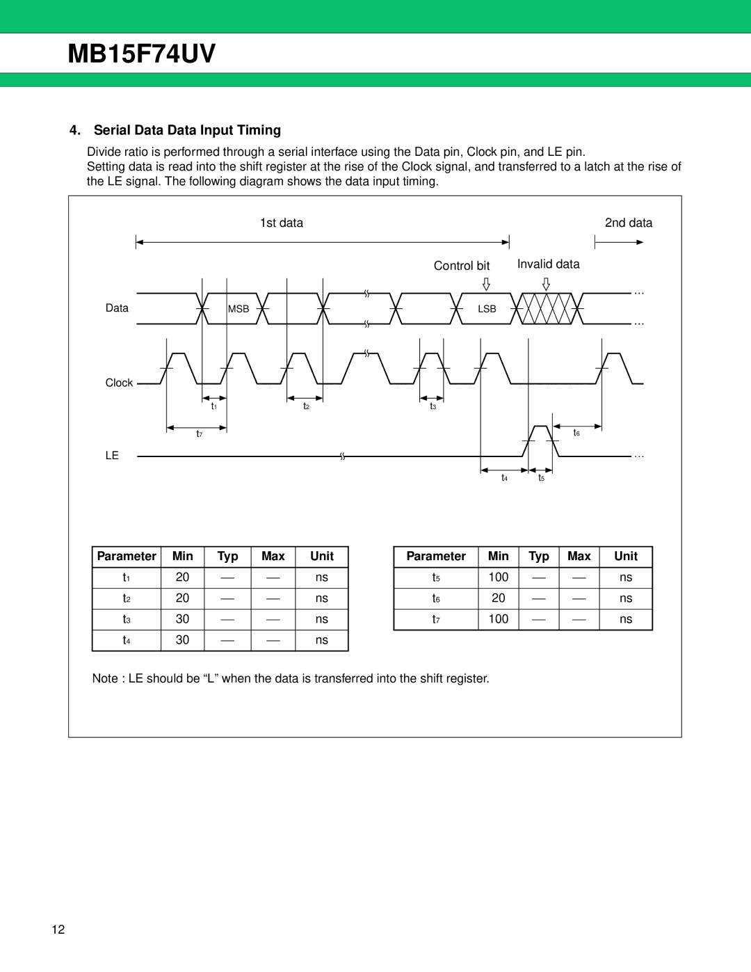
Divide ratio is performed through a serial interface using the Data pin, Clock pin, and LE pin.
Setting data is read into the shift register at the rise of the Clock signal, and transferred to a latch at the rise of the LE signal. The following diagram shows the data input timing.
1st data |
| 2nd data | |
|
|
|
|
Control bit | Invalid data | ||
Data
Clock
LE
t1
t7
MSB
t2
LSB
t3
t6
t4t5
Parameter | Min | Typ | Max | Unit |
|
|
|
|
|
t1 | 20 | | | ns |
|
|
|
|
|
t2 | 20 | | | ns |
|
|
|
|
|
t3 | 30 | | | ns |
|
|
|
|
|
t4 | 30 | | | ns |
|
|
|
|
|
Parameter | Min | Typ | Max | Unit |
|
|
|
|
|
t5 | 100 | | | ns |
|
|
|
|
|
t6 | 20 | | | ns |
|
|
|
|
|
t7 | 100 | | | ns |
|
|
|
|
|
Note : LE should be “L” when the data is transferred into the shift register.
12