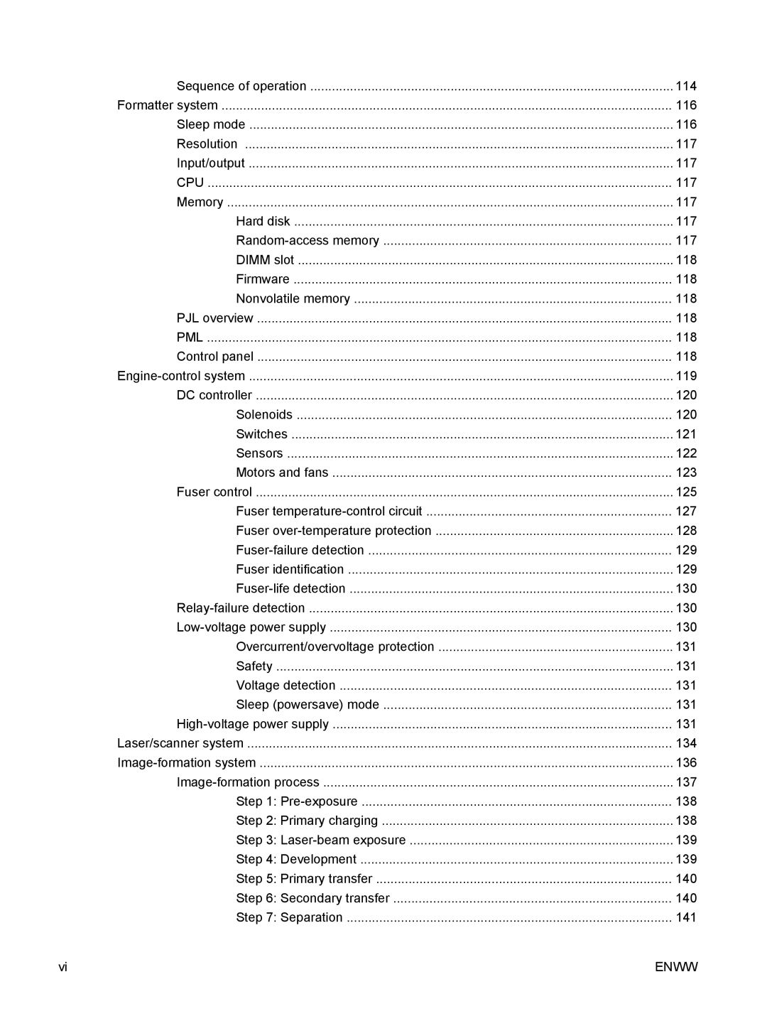
Sequence of operation | 114 |
Formatter system | 116 |
Sleep mode | 116 |
Resolution | 117 |
Input/output | 117 |
CPU | 117 |
Memory | 117 |
Hard disk | 117 |
117 | |
DIMM slot | 118 |
Firmware | 118 |
Nonvolatile memory | 118 |
PJL overview | 118 |
PML | 118 |
Control panel | 118 |
119 | |
DC controller | 120 |
Solenoids | 120 |
Switches | 121 |
Sensors | 122 |
Motors and fans | 123 |
Fuser control | 125 |
Fuser | 127 |
Fuser | 128 |
129 | |
Fuser identification | 129 |
130 | |
130 | |
130 | |
Overcurrent/overvoltage protection | 131 |
Safety | 131 |
Voltage detection | 131 |
Sleep (powersave) mode | 131 |
131 | |
Laser/scanner system | 134 |
136 | |
137 | |
Step 1: | 138 |
Step 2: Primary charging | 138 |
Step 3: | 139 |
Step 4: Development | 139 |
Step 5: Primary transfer | 140 |
Step 6: Secondary transfer | 140 |
Step 7: Separation | 141 |
vi | ENWW |
