SECTION 4 CIRCUIT DESCRIPTION
4-1 RECEIVER CIRCUITS
4-1-1 ANTENNA SWITCHING CIRCUIT (MAIN UNIT)
The antenna switching circuit functions as a
Received signals enter the antenna connector (CHASSIS; J1) and pass through the
4-1-2 RF CIRCUIT (MAIN UNIT)
The RF circuit amplifies signals within the range of frequen- cy coverage and filters
The signals from the antenna switching circuit pass through the
D4,
4-1-3 1ST MIXER AND 1ST IF CIRCUITS (MAIN UNIT)
The 1st mixer circuit converts the received signal into fixed frequency of the 1st IF signal with the PLL output frequency. By changing the PLL frequency, only the desired frequency passes through a crystal filter at the next stage of the 1st mixer.
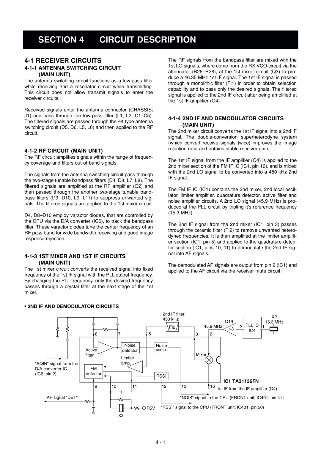
• 2ND IF AND DEMODULATOR CIRCUITS
The RF signals from the bandpass filter are mixed with the 1st LO signals, where come from the RX VCO circuit via the attenuator
4-1-4 2ND IF AND DEMODULATOR CIRCUITS (MAIN UNIT)
The 2nd mixer circuit converts the 1st IF signal into a 2nd IF signal. The
The 1st IF signal from the IF amplifier (Q4) is applied to the 2nd mixer section of the FM IF IC (IC1, pin 16), and is mixed with the 2nd LO signal to be converted into a 450 kHz 2nd IF signal.
The FM IF IC (IC1) contains the 2nd mixer, 2nd local oscil- lator, limiter amplifier, quadrature detector, active filter and noise amplifier circuits. A 2nd LO signal (45.9 MHz) is pro- duced at the PLL circuit by tripling it’s reference frequency (15.3 MHz).
The 2nd IF signal from the 2nd mixer (IC1, pin 3) passes through the ceramic filter (FI2) to remove unwanted hetero- dyned frequencies. It is then amplified at the limiter amplifi- er section (IC1, pin 5) and applied to the quadrature detec- tor section (IC1, pins 10, 11) to demodulate the 2nd IF sig- nal into AF signals.
The demodulated AF signals are output from pin 9 (IC1) and applied to the AF circuit via the receiver mute circuit.
"SQIN" signal from the D/A converter IC (IC6, pin 2)
AF signal "DET"
![]() 8
8
Active filter
FM
detector
9
| 2nd IF filter |
|
|
|
|
|
|
|
|
|
| X2 | |||||
| 450 kHz |
|
|
|
| Q19 |
|
|
|
|
| ||||||
|
|
|
|
|
|
|
| 15.3 MHz | |||||||||
|
|
|
|
| 45.9 | MHz |
|
| PLL IC | ||||||||
|
| FI2 |
|
| ⋅3 | 2 |
| 1 |
|
|
|
|
| ||||
|
|
|
|
|
|
|
| ||||||||||
7 | 5 |
|
| 3 |
| 2 |
|
|
|
| IC4 |
|
|
|
|
|
|
|
|
|
|
|
|
|
|
|
|
|
|
| |||||
|
|
|
|
|
|
|
|
|
|
| |||||||
|
|
|
|
|
|
|
|
|
|
|
|
|
|
|
|
|
|
| Noise | Noise |
|
|
| detector | comp. |
| Mixer |
| Limiter |
|
| |
|
|
|
| |
| amp. |
|
|
|
|
| RSSI |
| IC1 TA31136FN |
|
|
|
| |
10 | 11 | 12 | 13 | 16 1st IF from the IF amplifier (Q4) |
|
|
| "NOIS" signal to the CPU (FRONT unit; IC401, pin 41) | |
| R5V | "RSSI" signal to the CPU (FRONT unit; IC401, pin 50) | ||
X2
4 - 1