January
536EX Chipset
Developer’s Manual
Intel Confidential
536EX Chipset Developer’s Manual
Contents
Contents
Figures
Tables
Revision
Revision History
Date
Description
Introduction
1.1Controllerless Modem Driver Overview
User applications
Figure 1. WDM Driver Block Diagram
1.1.2Windows 95 and Windows
Kernel - ring0
Figure 2. VxD Mini Port Driver Block Diagram
1.2V.90/V.92 and V.34 Data Modes
1.3Modem Connection Overview
Table 3. DCE-to-ISPData Rates for V.90 Mode
Table 1. DTE-to-DCEData Rates for Each Mode
Table 2. DCE-to-DCEData Rates for Each Mode
1.4.1Sending Commands
Table 4. DTE-ModemData Rate Response Codes
1.4.2AT Escape Sequences
1.4.3Dial Modifier
Table 5. Data Mode Command Summary
AT Command Summary Tables
AT Command Summary Tables
Table 5. Data Mode Command Summary Continued
Result code type
Intel Confidential
Generate data mode calling tone
Table 6. V.44/V.42/V.42 bis MNP Command Summary
connect state, transmits
Table 7. Fax Identity Command Summary
Table 8. Fax Class 1 Command Summary
Table 9. IS-101Voice Command Summary
Table 10. Voice DTE→DCE Character Pairs
Table 10. Voice DTE→DCE Character Pairs Continued
Table 11. Voice DTE←DCE Character Pairs
Table 13. S-RegisterSummary
Table 11. Voice DTE←DCE Character Pairs Continued
Table 12. Dial Modifiers
Table 13. S-RegisterSummary Continued
Data Mode AT COMMANDS
Data Mode AT COMMANDS
ATW0
Table 14. Data Reporting Wn Mapping
Figure 3. Example of a Remote Connection
•ATW2
Examples
+FMFR?, +FMDL?, +FREV?
3.8Modem-to-ModemConnection Data Rates
3.6Online Command Mode Escape Codes, On
3.7Hanging Up Hn, S10, Zn, &D2
536EX Chipset Developer’s Manual
+VCID=1
+PMH=0
+PCW=0
+++AT
536EX Chipset Developer’s Manual
hook to connect the call. Now you can answer the phone and talk. After completing your voice conversation, the modem will issue another +PMHF and ATO command to initiate a Quick Connect. If the server rejects the request to go on hold, the user can stay on line ATO command issued or disconnect from his initial data connection ATH command issued
Table 16. Supported Modulation Types
3.9Diagnostic Testing S18, &Tn
3.9.1Local Analog Loopback AT&T1
Figure 6. Local Analog Loopback Test
3.9.2Local Analog Loopback With Self-TestAT&T8
LOCAL MODEM
Local Modem or Test Modem
3.10.1Time-IndependentEscape Sequence
Licensing Requirements for Hayes Escape Sequence
char1 = char2 = char3 = escape character S2
<char1><char2><char3><AT command><contents of S3>
Format
Table 18. Data Mode Command Descriptions
3.10.2Hayes* Escape Sequence
536EX Chipset Developer’s Manual
Sn=x
536EX Chipset Developer’s Manual
Data Mode AT COMMANDS
Intel Confidential
Intel Confidential
AT&V0
536EX Chipset Developer’s Manual
Definition
Command Default
Indication
1, 0,
536EX Chipset Developer’s Manual
1, 1,
+ESR
+ETBM
+IFC
+GMR
+GSN
+ILRR=m
modulations
+MS=m
<carrier>
Description
see ‘m’
<value>
+PHSW=
+PMHF
+PMHR
536EX Chipset Developer’s Manual
Table 19. Operating Modes
Error Correction and Data Compression4
Error Correction and Data Compression
Table 20. Resulting +ES Connection Types
NOTES
536EX Chipset Developer’s Manual
Error Correction and Data Compression
Intel Confidential
536EX Chipset Developer’s Manual
+DS=m
+DR=m
direction
<max string>
3768
+EFCS=m
+ER=m
+ES=m
5.2Fax Class 1 Commands
Fax Class 1 AT Commands
5.1Fax Identity Commands
Fax Class 1 AT Commands
Table 23. <mod> Selection Table
Figure 8. T.30 HDLC Frame Format
Table 24. Fax Mode Command Descriptions
Refer to Table 23 on page
Table 24. Fax Mode Command Descriptions Continued
+FRH=m
shown in Table 23 on page
+FTH=m
IS-101Voice Mode AT Commands
IS-101Voice Mode AT Commands
6.2Relay Control
Table 25. Voice Mode Command Descriptions
6.1DTMF Detection Reporting
+FLO=m
m = <deassert>, <assert>
m=<enable>, <report>
+VDR=m
m = <mask>
+VEM=m
Intel Confidential
+VIP
Preassigned Voice I/O Labels
+VLS=m
Voice I/O Primitive Codes
Relay/Playback Control: cont
+VSD=m
+VRX
m = <sds>, <sdi>
Transmission: Range:
m= <cml>, <vsr>, <scs>, <sel>
+VSM=m
Compression Method Selection: cont
+VSP=m
factory default is ‘0’
+VTS=m
none
Description
Command
Default
DTMF and Tone Generation: cont
S-Registers
S-Registers
Table 26. S-RegisterCommand Descriptions
536EX Chipset Developer’s Manual
Intel Confidential
S-Registers
536EX Chipset Developer’s Manual
Intel Confidential
S-Registers
536EX Chipset Developer’s Manual
Intel Confidential
S-Registers
536EX Chipset Developer’s Manual
Table 27. Caller ID Tags for Formatted Reporting
Caller ID
Caller ID
<DLE> R
RING DATE = TIME = NMBR = NAME = DOE JOHN MESG =
RING RING
NMBR =
Parallel Host Interface 16C450/16C550A UART
Parallel Host Interface 16C450/16C550A
UART
Figure 11. UART Emulation in Intelsdb.VxD
UART Transmitter Flow Diagram
UART Receiver Flow Diagram
ADDRESS
REGISTER
BIT NUMBER
NAME
Figure 14. Scratch Register SCR
9.2.1Scratch Register SCR
9.2.2Modem Status Register MSR
Figure 15. Modem Status Register MSR
9.2.3Line Status Register LSR
Figure 16. Line Status Register LSR
Figure 17. Modem Control Register MCR
9.2.4Modem Control Register MCR
9.2.5Line Control Register LCR
Figure 18. Line Control Register LCR
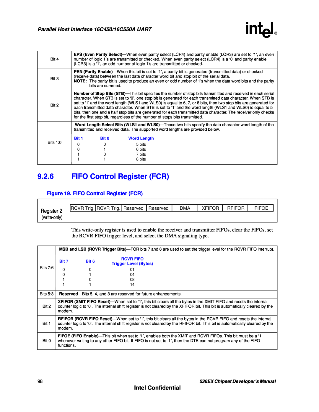
Figure 19. FIFO Control Register FCR
9.2.6FIFO Control Register FCR
Register
Table 28. Interrupt Control Functions
9.2.7Interrupt Identity Register IIR
Figure 20. Interrupt Identity Register IIR
9.2.9Transmitter Holding Register THR
9.2.8Interrupt Enable Register IER
Figure 21. Interrupt Enable Register IER
Figure 22. Transmitter Holding Register THR
Figure 23. Receiver Buffer Register RBR
9.2.10Receiver Buffer Register RBR
9.2.11Divisor Latch Registers DLM and DLL
Figure 24. Divisor Latch Registers DLM and DLL
9.3.2FIFO Polled Mode Operation
9.316C550A UART FIFO Operation
9.3.1FIFO Interrupt Mode Operation
536EX Chipset Developer’s Manual
Intel Confidential
Parallel Host Interface 16C450/16C550A UART