Intel Server Board SE7501WV2
Intel reference number C25653-001
Revision
Revision History Intel Server Board SE7501WV2 TPS
Date Revision Modifications Number
Table of Contents
Server Management
Table of Contents Intel Server Board SE7501WV2 TPS
Intel Server Board SE7501WV2 TPS Table of Contents
Bios
Revision Intel reference number C25653-001
12.1
Revision Vii Intel reference number C25653-001
FRB3
FRB2
Viii
SE7501WV2 Acpi Implementation 136
SE7501WV2 Connectors 139
General Specifications 159
Configuration Jumpers 157
164
Regulatory and Integration Information
167
Mechanical Specifications
169
Appendix a Glossary
List of Figures Intel Server Board SE7501WV2 TPS
Xii Revision Intel reference number C25653-001
Xiii
Intel Server Board SE7501WV2 TPS List of Tables
List of Tables Intel Server Board SE7501WV2 TPS
Xiv Revision Intel reference number C25653-001
Interrupt 15h Extensions 127
Xvi Revision Intel reference number C25653-001
Intel Server Board SE7501WV2 TPS Introduction
Bios
SE7501WV2 Server Board Overview Intel Server Board SE7501WV2
SE7501WV2 Feature Set
Revision Intel reference number C25653-001
Intel Server Board SE7501WV2 Block Diagram
Processor Support
Processor and Memory Subsystem
Processor VRM
Functional Architecture Intel Server Board SE7501WV2
Cache 400MHz Spec Size
Memory Subsystem
Reset Configuration Logic
Processor Module Presence Detection
Interrupts and Apic
Memory Dimm Support
Memory Configuration
Memory Dimm Bank
Memory Bank Labels
Bank
2.3 I2C*Bus
Dimm Failure LED
Intel E7501 Chipset
Intel Single Device Data Correction feature
DDR Configurations
MCH Memory Architecture
MCH North Bridge
3 P64H2
Configuration
PCI Bus P64-B I/O Subsystem
PCI Bus P64-C I/O Subsystem
4 ICH3-S
P64-C Speeds
Functional Architecture Intel Server Board SE7501WV2 TPS
PCI Bus Master IDE Interface
PCI Bus P32-A I/O Subsystem
USB Interface
Compatibility Interrupt Control
Super I/O
Power Management
GPIOs
Apic
Serial Ports
Serial Port a
Pin Signal Name Serial Port a Header Pin-out
Serial Port B
Serial Port Multiplexer Logic
Rear RJ45 Serial B Port
Pin 1 DCD to Pin #7
RJ45 Signal Abbr
Pin 1 DSR to Pin#7
Rear Serial Port B Adapter Pinout
Floppy Disk Controller
Bios Flash
Keyboard and Mouse
Wake-up Control
Memory Shadowing
Main Memory
System Management Mode Handling
Accessing Configuration Space
Configaddress Register
I/O Map
Reserved Bus Number Device
Register Enable bit ‘1’ = enabled, ‘0’ = disabled
Bus Number
Device Number and Idsel Mapping
Hardware Initialization
Clock Generation and Distribution
Scsi
Revision
Intel Server Board SE7501WV2 Clock Distribution
PCI Subsystem
PCI I/O Subsystem
2 P32-A 32-bit, 33-MHz PCI Subsystem
Device IDs Idsel
P64-C Configuration IDsIDs
P64-B Configuration IDs
Baseboard Signals Device
3 P64-B and P64-C 64-bit, 100-MHz PCI-X Subsystem
3.3 P64-C Arbitration
3.2 P64-B Arbitration
Zero Channel RAID ZCR Capable Riser Slot
P64-B Arbitration Connections
ATA-100
Ultra320 Scsi
Video Modes
Video Controller
Video Memory Interface
Signal Name Type Description
Video Modes
Video Memory Interface
Network Interface Controller NIC
NIC Connector and Status LEDs
Interrupt Routing
Front Panel Video Memory
Serialized IRQ Support
Legacy Interrupt Routing
Apic Interrupt Routing
Legacy Interrupt Sources
Intel Server Board SE7501WV2 Interrupt Mapping
Device PCI Riser Connector PCI Riser Slot Other
P64H2 Ch a
P64H2 Ch B
IRQ12 IRQ13 IRQ14 IRQ15
Server Management Intel Server Board SE7501WV2 TPS
Intel Server Board SE7501WV2 Sahalee BMC Block Diagram
Sahalee Baseboard Management Controller BMC
Pin # Pin Name Signal Type Description Config
BMC Pinout
Intel Server Board SE7501WV2 TPS Server Management
XINT5 ICH3SMIBUFFL
XINT4 NIC1SMBALERTL
XINT6 BMCPCU12PROCHOTL
XINT7 Bmcnmil
ADDR8
CTS1 Nsibmcfrcupdatel
ADDR9
ADDR10
LED2 Zzspaswitchen
LED1 Zzbmcrollingbiosl
RTS1 Bmcicmbtxenb L
BMC
VDD5V SB5V
Avdd SB5V
Iovcc SB3V
Corevcc SB3V
ADM1026 Input Definition
Fault Resilient Booting
FRB-1
FRB-2
Power-up Reset
System Reset Control
Hard Reset
FRB-3
Intelligent Platform Management Buses Ipmb
Soft Reset
Inter Chassis Management Bus Icmb
Intel Server Board SE7501WV2 I2C Address Map
Error Reporting
CPU LEDs
Dimm LEDs
Fan LEDs
5.4 5VSB Status LED
Non-Critical Condition
Degraded Condition
ID LED
Boot Block Post Progress Codes
Post Code Diagnostic LEDs
Diagnostic LED Description Decoder
Low
Off Read Microcode updates from Bios ROM
6Ah Off Initialize language module. Display splash logo
Temperature Sensors
System Flash ROM Layout
Bios Boot Specification Compliance
Memory
Memory Sizing and Initialization
Memory Configuration
Processors
Extended System Configuration Data ESCD, Plug and Play PnP
ECC Initialization
Memory Remapping
Resource Allocation
PnP ISA Auto-Configuration
Legacy ISA Configuration
PCI Auto-Configuration
Automatic Detection of Video Adapters
Boot without Keyboard and/or Mouse
Keyboard / Mouse Configuration
Floppy Drives
Allowed Combinations of Floppy Drive and Floppy Media
Bios Supported Server Management Features
Universal Serial Bus USB
Ipmi
Advanced Configuration and Power Interface Acpi
Power Switch Off to On
Front Panel Switches
Wake Events
Supported Wake Events
On to Off Legacy
Wired For Management WFM
On to Off Acpi
On to Sleep Acpi
Bios Recommendations
PXE Bios Support
Bios Requirements
Console Redirection
Keystroke Mappings
Operation
Non-ASCII Key Mappings
Key
VT100+ Shift Ctrl Alt
ESCO1
Escoz
Esca
Escb
Limitations
Ascii Key Mappings
Key Normal Shift Ctrl Alt
Service Partition Boot
Interaction with Bios Console Redirection
Emergency Management Port EMP
System Management Bios Smbios
Structure Type Supported Comments
Smbios Header Structure
Microsoft* Windows* Compatibility
Bios Serviceabilty Features
Quiet Boot
Cmos Reset
Flash Update Utility
Bios Updates
Bios Recovery Mode
Loading the System Bios
Performing Bios Recovery
User Binary Area
Rolling Bios and On-line updates
Bios Setup Utility
Bios and System Setup
Setup Utility Operation
Keyboard Command Bar
Entering the Bios Setup Utility
Setup Utility Screen
Keyboard Command Bar
Intel Server Board SE7501WV2 TPS Key Option Description
Menu Selection Bar
Main Menu Selections
Feature Option Description
Main Menu Selections
44 / 1.2 MB 3½
Advanced Menu Selections
Processor Settings Sub-menu
Primary Master and Slave Adapters Sub-menu Selections
100 Revision Intel reference number C25653-001
Advanced Menu Selections
PCI Configuration Sub-menu Selections
Advanced Chipset Control Sub-menu Selections
Revision 101 Intel reference number C25653-001
PCI Device, Embedded Devices
O Device/Peripheral Configuration Sub-menu Selections
102 Revision Intel reference number C25653-001
3F8h
Security Menu Selections
Memory Configuration Menu Selections
Security Menu Selections
Revision 103 Intel reference number C25653-001
Server Menu Selections
Server Menu Selections
104 Revision Intel reference number C25653-001
System Management Sub-menu Selections
Revision 105 Intel reference number C25653-001
Retry 3 times
Event Log Configuration Sub-menu Selections
Serial Console Redirection Sub-menu Selections
106 Revision Intel reference number C25653-001
Fault Resilient Boot Sub-menu Selections
Boot Menu Selections
Boot Menu Selections
Boot Device Priority Selections
Hard Drive Selections
Exit Menu Selections
Removable Devices Selections
Exit Menu Selections
Security Features Operating Model
Bios Security Features
Mode Entry Method Behavior Exit Criteria After Exit Event
Operating Model
110 Revision Intel reference number C25653-001
Password Protection
Password Clear Jumper
Inactivity Timer
Secure Mode Unattended start
Hot Key Activation
Error Handling
Secure Boot Unattended Start
29 PS/2 Keyboard and Mouse Lock
112 Revision Intel reference number C25653-001
Processor Bus Error
PCI Bus Error
Single-Bit ECC Error Throttling Prevention
SMI Handler
Boot Event
System Limit Error
Fault Resilient Booting FRB
38.1 FRB3
Revision 115 Intel reference number C25653-001
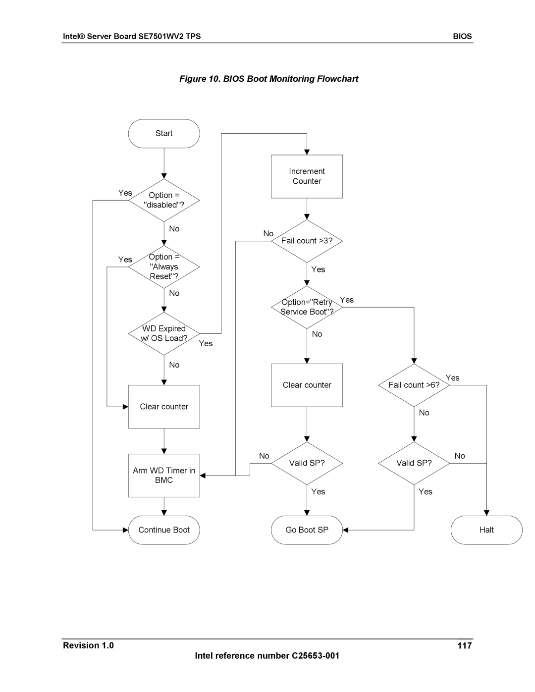
Boot Monitoring
Purpose
116 Revision Intel reference number C25653-001
Revision 117 Intel reference number C25653-001
Bios Boot Monitoring Flowchart
Memory Error Events
Logging Format Conventions
118 Revision Intel reference number C25653-001
Memory Error Event Data Field Contents
PCI Error Event Data Field Contents
PCI Error Events
FRB-2 Error Events
Examples of Event Data Field Contents for PCI Errors
FRB-2 Event Data Field Contents
Post Codes, Error Messages, and Error Codes
Examples of Event Data Field Contents for FRB-2 Errors
Post Progress Code LEDs
Standard Post Error Messages and Codes
Post Error Codes and Messages
Error Code Error Message Pause on Boot
Revision Intel reference number C25653-001 123
124 Revision Intel reference number C25653-001
Extended Post Error Messages and Codes
Bios Recovery Beep Codes
Post Error Beep Codes
Bios Recovery Beep Codes
Beeps Error Post Progress Code Description Message
Bootblock Error Beep Codes
Bootblock Error Beep Codes
Three-beep Boot Block Memory Failure Error Codes
126 Revision Intel reference number C25653-001
43 SE7501WV2 Server Board Bios Runtime APIs
Post Error Pause Option
Cache Services
INT 15 Extensions
Intel ID String
128 Revision Intel reference number C25653-001
Esdi
Extended Nvram Services
Processor Information
Revision 129 Intel reference number C25653-001
Multiprocessor Specification Support
Ipmb Services
Multiple Processor Support MPS
130 Revision Intel reference number C25653-001
Multiple Processor Support
Mixed Processor Support
Revision 131 Intel reference number C25653-001
OEM Customization
Hyper-Threading Technology
User Binary
132 Revision Intel reference number C25653-001
Revision 133 Intel reference number C25653-001
User Binary Area Scan Point Definitions
Scan Point Definitions
134 Revision Intel reference number C25653-001
Scan Point Mask RAM/Stack/BDA Video/Keyboard
OEM Splash Screen
Format of the User Binary Information Structure
Localization
User Binary Information Structure
136 Revision Intel reference number C25653-001
Acpi
Revision 137 Intel reference number C25653-001
138 Revision Intel reference number C25653-001
Wake up Sources Acpi and Legacy
Power Connector Pin-out J3J1
Power Connectors
Power Supply Signal Connector J1J1
Power Connector J4J1
Dimm Connectors J5F1, J5F2, J5F3, J6F1, J6F2, J6F3
Memory Module Connector
SE7501WV2 Connectors Intel Server Board SE7501WV2 TPS
140 Revision Intel reference number C25653-001
Socket 604 Processor Socket Pinout
Processor Socket
Revision 141 Intel reference number C25653-001
Pin Pin Name
142 Revision Intel reference number C25653-001
System Management Headers
PCI I/O Riser Slot Connector
Icmb Header
OEM Ipmb Header
144 Revision Intel reference number C25653-001
P64-C Low-Profile Riser Slot Pin-out
Pin Side B Side a Connector Key
Revision 145 Intel reference number C25653-001
IRQ4 TDI IRQ0 IRQ3 IRQ1 PRSNT1# REQ3# GNT2# PRSNT2# GNT3#
Pin Front Panel Connector Signal Descriptions
Front Panel Connectors
Signal Type Description
146 Revision Intel reference number C25653-001
SSI Compliant 24-pin Front Panel Connector Pinout J1H1
Pin Signal Name
148 Revision Intel reference number C25653-001
Revision 149 Intel reference number C25653-001
Scsi Connectors
VGA Connector
VGA Connector Pin-out J8A1
Pin Vhdci Scsi and Wide Connectors Pin-out J7B1, J7A1
NIC Connector
Stacked Dual RJ-45 Connector Pin-out JA6A1
Revision 151 Intel reference number C25653-001
ATA-100 RAID 40-pin Connectors Pin-out J1D1, J1D2
ATA RAID Connectors
152 Revision Intel reference number C25653-001
IDEA1 Diag IDEA0 IDEA2 IDEDCS0L IDEDCS1L Idehdactl GND
ATA-100 Legacy 40-pin Connector Pinout J1G2
USB Connector
USB Connectors Pin-out J4A1, J9A1
Revision 153 Intel reference number C25653-001
Legacy 34-pin Floppy Connector Pin-out J1G1
Floppy Connector
SE7501WV2 ConnectorsIntel Server Board SE7501WV2 TPS
Optional USB Connection Header Pin-out J1D3
Keyboard and Mouse Connector
Serial Port Connector
Rear Low-Profile RJ-45 Serial B Port Pin-out J5A1
Pin Header Serial a Port Pin-out J9A2
Miscellaneous Headers
Keyboard and Mouse PS/2 Connector Pin-out J6A1
Fan Headers
Three-pin Fan Headers Pin-out J4J2, J7J1
Configuration Jumper Options
System Recovery and Update Jumpers
Intel Server Board SE7501WV2 TPS Configuration Jumpers
Revision 157 Intel reference number C25653-001
Configuration Jumpers Intel Server Board SE7501WV2 TPS
External RJ45 Serial Port Jumper Block
158 Revision Intel reference number C25653-001
10.2.1 SE7501WV2 Server Board Power Budget
Power Information
Intel Server Board SE7501WV2/SR2300/SR1300 Power Budget
Absolute Maximum Ratings
Power Timing
Power Supply Specifications
160 Revision Intel reference number C25653-001
Parameter Min Nom Max Units Tolerance
Turn On / Off Timing
Voltage Timing Parameters
Revision Intel reference number C25653-001 161
Description Min Max Units
1000 Msec Regulation at AC turn on
162 Revision Intel reference number C25653-001
Revision 163 Intel reference number C25653-001
Voltage Recovery Timing Specifications
Product Regulatory Compliance
Product Safety Compliance
Product EMC Compliance
Product Regulatory Compliance Markings
Electromagnetic Compatibility Notices
Replacing the Back up Battery
Europe CE Declaration of Conformity
Bsmi Taiwan
166 Revision Intel reference number C25653-001
Varning
Revision 167 Intel reference number C25653-001
Intel Server Board SE7501WV2 TPS Mechanical Specifications
PCI Riser Cards
Mechanical Specifications Intel Server Board SE7501WV2 TPS
12.1.1 1-Slot 3.3V PCI Riser Card
12.1.2 3-Slot 3.3V PCI Riser Card
Revision 169 Intel reference number C25653-001
Intel Server Board SE7501WV2 TPS Appendix a Glossary
Term Definition
170 Revision Intel reference number C25653-001