CV-M4+/M4+CL, CV-M7+/M7+CL
5. Pin Assignment
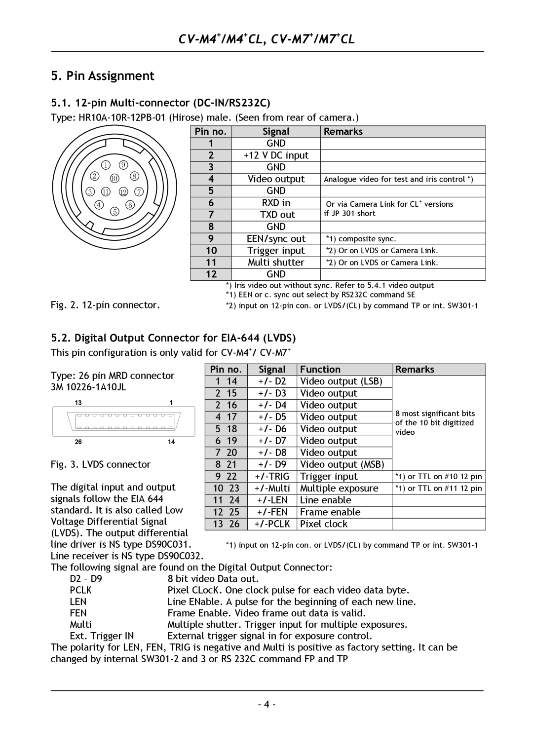
5.1. 12-pin Multi-connector (DC-IN/RS232C)
Type:
1 9
2 10 8
3 11 12 7
46
5
Fig. 2. 12-pin connector.
Pin no. | Signal | Remarks |
1GND
2+12 V DC input
3GND
4Video output Analogue video for test and iris control *)
5GND
| 6 |
| RXD in | Or via Camera Link for CL+ versions |
| 7 |
| TXD out | if JP 301 short |
8GND
9 | EEN/sync out | *1) composite sync. |
10Trigger input *2) Or on LVDS or Camera Link.
11Multi shutter *2) Or on LVDS or Camera Link.
12GND
*) Iris video out without sync. Refer to 5.4.1 video output *1) EEN or c. sync out select by RS232C command SE
*2) input on
5.2.Digital Output Connector for EIA-644 (LVDS)
This pin configuration is only valid for
Type: 26 pin MRD connector | Pin no. |
|
| Signal |
|
| Function |
|
| Remarks |
| ||||||||||||||||||||||||||||||
1 | 14 |
|
| +/- D2 |
| Video output (LSB) |
|
|
|
| |||||||||||||||||||||||||||||||
3M |
|
|
|
|
|
|
|
|
|
|
| ||||||||||||||||||||||||||||||
|
|
|
| 2 | 15 |
|
| +/- D3 |
|
| Video output |
|
|
|
| ||||||||||||||||||||||||||
13 |
|
|
|
|
|
|
|
|
|
|
|
|
|
|
|
|
|
|
|
|
|
| 1 |
|
|
|
|
|
|
|
|
| |||||||||
|
|
|
|
|
|
|
|
|
|
|
|
|
|
|
|
|
|
|
|
|
|
| 2 | 16 |
|
| +/- D4 |
|
| Video output |
|
| 8 most significant bits |
| |||||||
|
|
|
|
|
|
|
|
|
|
|
|
|
|
|
|
|
|
|
|
|
|
|
|
|
|
|
|
|
| 4 | 17 |
|
| +/- D5 |
|
| Video output |
|
|
| |
|
|
|
|
|
|
|
|
|
|
|
|
|
|
|
|
|
|
|
|
|
|
|
|
|
|
|
|
|
|
|
|
|
|
|
| of the 10 bit digitized |
| ||||
|
|
|
|
|
|
|
|
|
|
|
|
|
|
|
|
|
|
|
|
|
|
|
|
|
|
|
|
|
| 5 | 18 |
|
| +/- D6 |
|
| Video output |
|
|
| |
|
|
|
|
|
|
|
|
|
|
|
|
|
|
|
|
|
|
|
|
|
|
|
|
|
|
|
|
|
|
|
|
|
|
|
| video |
| ||||
|
|
|
|
|
|
|
|
|
|
|
|
|
|
|
|
|
|
|
|
|
|
|
|
|
|
|
|
|
|
|
|
|
|
|
|
| |||||
26 |
|
|
|
|
|
|
|
|
|
|
|
|
|
|
|
|
|
|
|
|
|
| 14 | 6 | 19 |
|
| +/- D7 |
|
| Video output |
|
|
|
| ||||||
|
|
|
|
|
|
|
|
|
|
|
|
|
|
|
|
|
|
|
|
|
|
|
|
|
|
|
|
|
| 7 | 20 |
|
| +/- D8 |
|
| Video output |
|
|
|
|
Fig. 3. LVDS connector |
|
|
|
| 8 | 21 |
|
| +/- D9 |
| Video output (MSB) |
|
|
|
| ||||||||||||||||||||||||||
The digital input and output | 9 | 22 |
|
|
| Trigger input |
|
| *1) or TTL on #10 12 pin |
| |||||||||||||||||||||||||||||||
10 | 23 |
|
|
| Multiple exposure |
|
| *1) or TTL on #11 12 pin |
| ||||||||||||||||||||||||||||||||
signals follow the EIA 644 |
|
|
|
| 11 | 24 |
|
|
| Line enable |
|
|
|
| |||||||||||||||||||||||||||
standard. It is also called Low | 12 | 25 |
|
|
|
| Frame enable |
|
|
|
| ||||||||||||||||||||||||||||||
Voltage Differential Signal |
|
|
|
| 13 | 26 |
|
|
|
| Pixel clock |
|
|
|
| ||||||||||||||||||||||||||
(LVDS). The output differential |
|
|
|
|
|
|
|
|
|
|
|
| |||||||||||||||||||||||||||||
line driver is NS type DS90C031. |
| *1) input on |
| ||||||||||||||||||||||||||||||||||||||
Line receiver is NS type DS90C032. |
|
|
|
|
|
|
|
|
|
|
|
| |||||||||||||||||||||||||||||
The following signal are found on the Digital Output Connector: |
|
|
|
| |||||||||||||||||||||||||||||||||||||
D2 – D9 | 8 bit video Data out. |
|
|
|
|
|
|
| |||||||||||||||||||||||||||||||||
PCLK | Pixel CLocK. One clock pulse for each video data byte. |
| |||||||||||||||||||||||||||||||||||||||
LEN | Line ENable. A pulse for the beginning of each new line. |
| |||||||||||||||||||||||||||||||||||||||
FEN | Frame Enable. Video frame out data is valid. |
|
|
|
| ||||||||||||||||||||||||||||||||||||
Multi | Multiple shutter. Trigger input for multiple exposures. |
| |||||||||||||||||||||||||||||||||||||||
Ext. Trigger IN | External trigger signal in for exposure control. |
|
|
|
| ||||||||||||||||||||||||||||||||||||
The polarity for LEN, FEN, TRIG is negative and Multi is positive as factory setting. It can be changed by internal
- 4 -