Internal Use Only
LG-C320
Table Of Contents
LGE Internal Use Only
Regulatory Information
Purpose
Electrostatic Sensitive Devices
Pictures
Interference and Attenuation
Abbreviations
PLL
PAM
PCB
PGA
Supporting Standard
Main Parts GSM Solution
Feature Comment
Product Name
HW Features
Stereo Headset Yes Data Cable Flash External Memory
Music Player
MP3/AAC/AAC+/WMA
Cdrom
SW Features
2M FF
MMS
Eons Cphs
ENS
HW Spec
GSM transceiver specification Specification
C320 Figures
General Description
QSC62703G disable Base band block
1 Processors and bus architecture
Processor
EBI2
Memory support and LCD interface
Qvga Main
QSC6270 3G disable
Connectivity
QSC6270
GPIOs
QSC6270 3G disable has 78 configurable I/O pins
JTAG/ETM
Enhanced GPS position location using gpsOne with RGR6240 IC
Air interfaces
Internal base band functions
Camera interface and video front-end
Multimedia
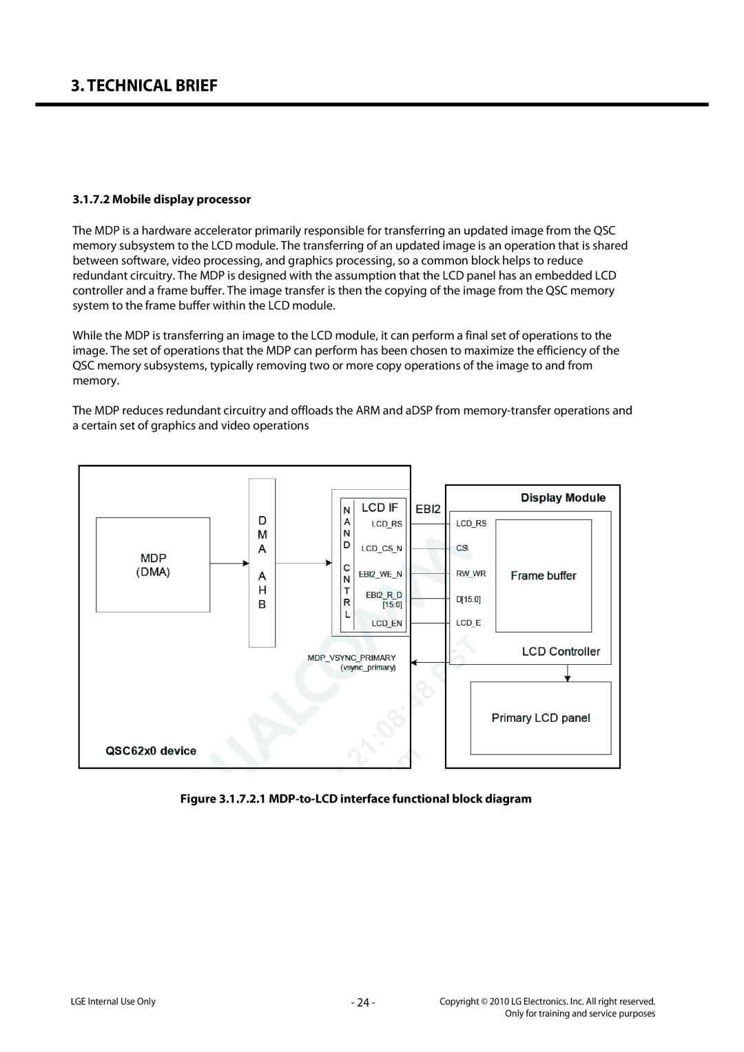
Mobile display processor
7.2.1 MDP-to-LCD interface functional block diagram
7.2.2 The LCD interface of C320
Hkadc
Uart
9 USB
QSC6270HKADC Block diagram
Valid external supply attachment and removal detection
Power management
Input power management
Output voltage regulation
2 Voltage regulator summary
Charging control
YlT
KEY PAD
Technical Brief SUB System
Sdram
EBI1 Features
EBI2 Features
External memory interface
3.1 2M Camera
Camera Interface 2M Camera
Technical Brief
General Description
LCD Module LQ024Q3UX01 Sharp
PIN Description
Input Signal and Power Pin Description Input Pin
Technical Brief
Audio Signal Processing & Interface
General Description RF Part
41 Block diagram of RF part
High-band
Low-band
GSM 850 869 to 894 MHz and GSM 900 925 to 960 MHz
1 QSC GSM receiver signal paths functional diagram
GSM Transmitter
1 D5008 FL101 FEM
1 Block diagram of FEM 1 Control table of FEM
2 Block diagram of GSM PAM
Shows the Bluetooth system architecture in the LG-C320
Bluetooth BCM2070
Bluetooth ConnectionGPIO with QSC6270
ESC6270
FM Receiver TEA5991
FM TEA5991
2 pin description
Than 3.20V? Yes
Power on Troubleshooting
When Power key press? Yes
Start
TP1
Yes Change TA Is it charging properly?
Charger Troubleshooting
Connection OK? Change I/O connector Yes
Charger Troubleshooting Flow
TP1 FL401
USB Troubleshooting Flow
USB Troubleshooting
TP3
Check J301
Usim Detect Troubleshooting
Re-insert the SIM card Work well ?
Yes Change the SIM card Work well ?
TP1 TP2
TP3
Camera Troubleshooting
TP4
CAM70MHz Pclk CAM24MHz Mclk
TP4 TP3 TP1 TP2
LED on ?
Main side view LED Troubleshooting
Check battery Change QSC6270 Change LED Yes
Key press +VPWR is above 3.2V? Yes
Slide Key side view LED Troubleshooting
SUB KEY B/L
Change SUB PCB LCD display OK? Yes
LCD Troubleshooting
Change the Fpcb Move to KEY LED Troubleshooting
LCD display OK? Yes
Slide Side view placement
Above 3.0V or Linmotm
Vibrator Troubleshooting
Vibrator is operate when DC motor driver is enabled
Main to Fsubfpcb ConnectorCN803
Fsubfpcb to Main PCB ConnectorCN101
Receiver Path
TP1
Main to Slide Fpcb ConnectorCN801
TP4Receiver PAD=CN101 TP3FB102 TP3FB101
Change the IC501
TP1C506, C507?
TP3FB505 TP3FB504 TP2R505 TP2R504
TP1C507 TP1C506
Speaker/Speaker Phone path
Audio Sub TP1C509 TP1C508 SystemIC501 TP2FB507 TP2FB508
TP3
TP4
TP5CN102=Speaker Pad
Work well?
Main microphone
Make a call
MICBIASTP1C526
Mainmicp
TP3C263? Yes
Headset microphone
Insert Headset & Make a call
TP2FB503? Yes
Hsgnd
U201 X202 FL101 SW101 U101
RF Component
GSM path
RF Path
GSM850/GSM900/1800/1900
Trouble Shooting of GSM Part
Check Rx Part Tx Part
Setup Test Equipnment Cell power = -74dbm
Egsm CH
DCS1800 CH PCS1900 CH GSM850 CH
Check U201 Replace FL101
Checking Front-End Module Block
TP1 TP2
GSM Rx is OK
Checking GSM Rx part
17.3 Gpam Logic Control
DCS/PCS =
Trouble Shooting
ANT
Checking Bluetooth Block
Bluetooth RF components
RF component BT Main board bottom Reference Description
Bluetooth Signal Path Main board bottom
Bluetooth Signal Path
TP4 Btantout
Bluetooth Trouble shooting
TP#
TP1 VREGMSMP2.6V TP2 VREGMSME1.8V TP3
ConnectivityANTPAD
BT main clk 26MHz
Class
Reference Description U701 TEA5991FM module
FM Signal Path
Checking FM Radio Block
FM Trouble shooting
TP1 VREGMSMP2.6V TP2 VREGMSME1.8V TP3 Fmantin TP4
Fmoutaudio signal
TP description
LG-C320
Download
LG-C320 LGE Internal Use Only
101
102
103
104
105
106
107
108
109
LG-C320 LG-C320
110
LG-C320 LG-C320
111
LG-C20
112
Block Diagram
Usbvbus
113
Vbat
114
Memory
115
116
117
118
ESC6270
119
120
WM9093
121
QSC6270
122
123
Circuit Diagram
124
2-1ESCESC6270
NET Conn
126
MCP2-12G1G DDRx16hynix
127
3-2
128
2-1
129
6CH+4LDO,PWM
130
ConnectivityANTPAD
131
1-1
132
1-3push1.50T
133
KEY PCB
134
Slide Fpcb
135
Module Fpcb
136
137
QSC6270 3G disableٛ- U200 bottom view
BGA Pin Map
138
H8BCS0SI0BAR-46M MCP,NAND U300 EUSY0347506
139
BCM2070B2KUBXG bluetooth U700 EUSY0418701
140
141
WM9093 Ultra Low Power Audio Subsystem- IC500 EUSY0403901
Bump CSP package Top View
142
TEA5991FM Tuner- U701 EUSY0385901
143
LD801/802 Main Key LED Can not use LED
U101 GSM PAM
IC401 Muic
FL101 FEM
145
C320KEYSPEY006820110TOP
146
CN102 LCD Connector Can not use LCD Display, LCD Backlight
147
C320FSLIDESPCY024690110TOP
148
CN101 Fpcb Conn Can not use SD-card, Vibrator, Speaker
149
Preparation work for setting RF cable loss
Procedure
Usage of Tachyon for RF Calibration and Test
150
Basic Setting of Tachyon for RF Calibration & Test
System Option Setting
Log of RF Calibration and Test
Contents
152
Phone Test Mode
153
Order
154
155
156
157
Exploded View & Replacement Part List
158
159
160
161
162
Mobitech Corporation
163
LGC320.ABOOWA Flexible
Hankook Molex
164
TP TDK Korea Cooperation
165
LG-C320 Boowa Main
RESIN,PC
Rohm
166
TP TDK Corporation
Kyocera Corp
167
AUK Corp
168
ESM R/TP 3P KEC Corporaition
169
FET
H8BCS0SI0BAR-46M NAND/2G SDRAM/1G 1.7VTO1.9V
170
IC,MCP,NAND
171
Printed Circuit Board Corp
QCT Skyworks Solutions INC
172
SPM0410LR5H-QB SPM0410LR5H-QB,UNIT,42
ECZH0001217
173
Ceratech Corporation
174
Microelectronics PLC
175
Accessory